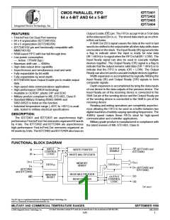
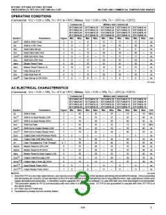
IDT72401, IDT72402, IDT72403, IDT72404
CMOS PARALLEL FIFO 64 x 4-BIT AND 64 x 5-BIT
MILITARY AND COMMERCIAL TEMPERATURE RANGES
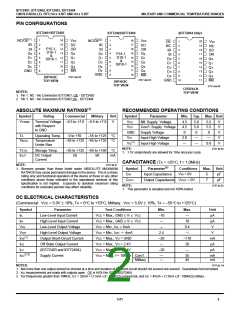
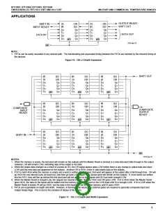
APPLICATIONS
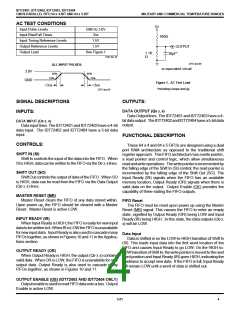
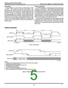
OUTPUT READY
SHIFT OUT
SHIFT IN
INPUT READY
SI
IR
D0
D1
D2
D3
OR
SO
Q0
Q1
Q2
Q3
SI
IR
D0
D1
D2
D3
OR
SO
Q0
Q1
Q2
Q3
DATA OUT
DATA IN
MR
MR
2747 drw 15
MR
NOTE:
1. FIFOs can be easily cascaded to any desired path. The handshaking and associated timing between the FIFOs are handled by the inherent timing of
the devices.
Figure 10. 128 x 4 Depth Expansion
SHIFT OUT
IR
SI
SO
OR
IR
SI
SO
OR
IR
SI
SO
OR
D
D1
D
D3
0
Q
Q
Q
Q
0
D
D1
D
D3
0
Q
Q
Q
Q
0
D
D1
D2
D3
0
Q
Q
Q
Q
0
1
2
3
1
2
3
1
2
3
2
2
MR
MR
MR
MR
MR
MR
MR
MR
MR
IR
SI
SO
OR
IR
SI
SO
OR
IR
SI
SO
OR
COMPOSITE
INPUT
COMPOSITE
OUTPUT
READY
D
0
Q
Q
Q
Q
0
D
0
Q
Q
Q
Q
0
D
0
Q
Q
Q
Q
0
READY
D1
D1
D1
D2
D3
1
2
3
1
2
3
1
2
3
D
2
D
2
D3
D3
IR
SI
SO
OR
IR
SI
SO
OR
IR
SI
SO
OR
SHIFT IN
D
0
Q
Q
Q
Q
0
D
0
Q
Q
Q
Q
0
D
0
Q
Q
Q
Q
0
D1
D1
D1
D2
D3
1
2
3
1
2
3
1
2
3
D
2
D
2
D3
D3
MR
2747 drw 16
NOTES:
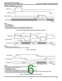
1. When the memory is empty, the last word will remain on the outputs until the Master Reset is strobed or a new data word falls through to the output.
However, OR will remain LOW, indicating data at the output is not valid.
2. When the output data changes as a result of a pulse on SO, the OR signal always goes LOW before there is any change in output data and stays
LOW until the new data has appeared on the outputs. Anytime OR is HIGH, there is valid stable data on the outputs.
3. If SO is held HIGH while the memory is empty and a word is written into the input, that word will appear at the output after a fall-through time. OR will
go HIGH for one internal cycle (at least tORL) and then go back LOW again. The stored word will remain on the outputs. If more words are written
into the FIFO, they will line up behind the first word and will not appear on the outputs until SO has been brought LOW.
4. When the Master Reset is brought Low, the outputs are cleared to LOW, IR goes HIGH and OR goes LOW. If SI is HIGH when the Master Reset
goes HIGH, the data on the inputs will be written into the memory and IR will return to the LOW state until SI is brought LOW. If SI is LOW when the
Master Reset is ended, IR will go HIGH, but the data in the inputs will not enter the memory until SI goes HIGH.
5. FIFOs are expandable on depth and width. However, in forming wider words, two external gates are required to generate composite Input and
Output Ready flags. This is due to the variation of delays of the FIFOs.
Figure 11. 192 x 12 Depth and Width Expansion
5.01
8

 IDT [ INTEGRATED DEVICE TECHNOLOGY ]