IDT72401, IDT72402, IDT72403, IDT72404
CMOS PARALLEL FIFO 64 x 4-BIT AND 64 x 5-BIT
MILITARY AND COMMERCIAL TEMPERATURE RANGES
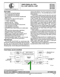
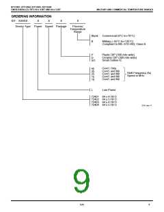
PIN CONFIGURATIONS
IDT72401/IDT72403
(IDT72404 Only)
IDT72402/IDT72404
NC/OE(1)
IR
Vcc
SO
OR
Q0
Q1
Q2
NC/OE(2)
Vcc
1
2
3
4
5
6
7
8
16
15
1
2
3
4
5
6
7
8
9
18
17
16
15
1
2
20
19
18
17
16
15
14
13
12
11
OE
NC
IR
SI
D0
D1
D2
D3
D4
Vcc
NC
SO
OR
Q0
Q1
Q2
Q3
Q4
MR
IR
SI
SO
OR
Q0
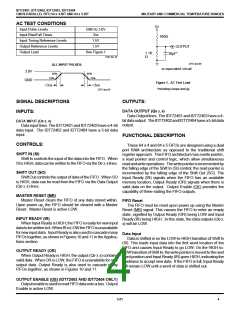
P16-1, 14
SI
D0
D1
D2
D3
3
D16-1
&
13
12
11
10
9
D0
D1
D2
P18-1,
4
D18-1 14
Q
1
5
S016-1
&
13
12
11
10
Q2
Q3
Q4
MR
6
S018-1
Q3
MR
D3
D4
GND
7
GND
8
9
2747 drw 02
DIP/SOIC
TOP VIEW
2747 drw 03
10
GND
DIP/SOIC
TOP VIEW
2747 drw 04
CERPACK
TOP VIEW
NOTES:
1. Pin 1: NC - No Connection IDT72401, OE - IDT72403
2. Pin 1: NC - No Connection IDT72402,OE - IDT72404
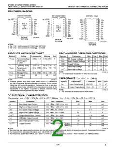
ABSOLUTE MAXIMUM RATINGS(1)
RECOMMENDED OPERATING CONDITIONS
Symbol
Parameter
Min. Typ. Max. Unit
Symbol
Rating
Commercial
Military
Unit
VTERM
Terminal Voltage –0.5 to +7.0 –0.5 to +7.0
with Respect
to GND
V
VCC
VCC
GND
VIH
Mil. Supply Voltage
Com'l. Supply Voltage
Supply Voltage
4.5
4.5
0
5.0
5.0
0
5.5
5.5
0
V
V
V
V
TA
Operating Temp.
0 to +70
–55 to +125 °C
Input High Voltage
2.0
—
—
TBIAS
Temperature
Under Bias
–55 to +125 –65 to +135 °C
(1)
VIL
Input High Voltage
—
—
0.8
V
NOTE:
2747 tbl 02
TSTG
IOUT
Storage Temp.
–55 to +125 –65 to +150 °C
1. 1.5V undershoots are allowed for 10ns once per cycle.
DC Output
Current
50
50
mA
CAPACITANCE (TA = +25°C, f = 1.0MHz)
NOTE:
2747 tbl 01
1. Stresses greater than those listed under ABSOLUTE MAXIMUM
RATINGS may cause permanent damage to the device. This is a stress
rating only and functional operation of the device at these or any other
conditions above those indicated in the operational sections of this
specification is not implied. Exposure to absolute maximum rating
conditions for extended periods may affect reliability.
Symbol
Parameter(1)
Conditions
Max. Unit
CIN
Input Capacitance
VIN = 0V
5
7
pF
pF
COUT
Output Capacitance VOUT = 0V
NOTE:
1. This parameter is sampled and not 100% tested.
2747 tbl 03
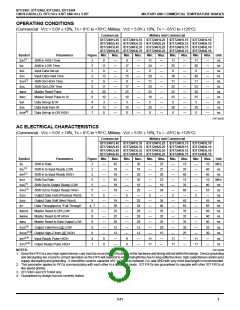
DC ELECTRICAL CHARACTERISTICS
(Commercial: VCC = 5.0V ± 10%, TA = 0°C to +70°C; Military: VCC = 5.0V ± 10%, TA = –55°C to +125°C)
Symbol
IIL
Parameter
Test Conditions
VCC = Max., GND ≤ VI ≤ VCC
VCC = Max., GND ≤ VI ≤ VCC
VCC = Min., IOL = 8mA
Min.
–10
—
Max.
—
Unit
Low-Level Input Current
High-Level Input Current
Low-Level Output Voltage
High-Level Output Voltage
Output Short-Circuit Current
Off-State Output Current
(IDT72403 and IDT72404)
Supply Current
µA
µA
V
IIH
10
VOL
VOH
—
0.4
—
VCC = Min., IOH = -4mA
VCC = Max., VO = GND
VCC = Max., VO = 2.4V
VCC = Max., VO = 0.4V
2.4
–20
—
V
(1)
IOS
–110
20
mA
µA
µA
IHZ
ILZ
–20
—
(2,3)
ICC
VCC = Max., f = 10MHz Com'l.
Military
—
—
35
45
mA
mA
NOTES:
2747 tbl 04
1. Not more than one output should be shorted at a time and duration of the short-circuit should not exceed one second. Guaranteed but not tested.
2. ICC measurements are made with outputs open. OE is HIGH for IDT72403/72404.
3
For frequencies greater than 10MHZ, ICC = 35mA + (1.5mA x [f - 10MHz]) commercial, and ICC = 45mA + (1.5mA x [f - 10MHz]) military.
5.01
2

 IDT [ INTEGRATED DEVICE TECHNOLOGY ]