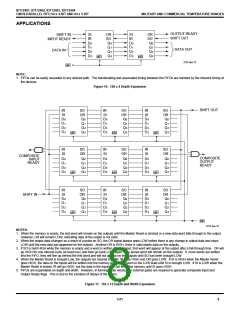
IDT72401, IDT72402, IDT72403, IDT72404
CMOS PARALLEL FIFO 64 x 4-BIT AND 64 x 5-BIT
MILITARY AND COMMERCIAL TEMPERATURE RANGES
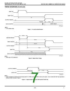
Data Output
Fall-Through Mode
The FIFO operates in a fall-through mode when data gets
Data is shifted out on the HlGH-to-LOW transition of Shift
Out (SO). This causes the internal read pointer to be shifted into an empty FIFO. After a fall-through delay the data
advanced to the next word location. If data is present, valid propagates to the output. When the data reaches the output,
data will appear on the outputs and Output Ready (OR) will the Output Ready (OR) goes HIGH. Fall-through mode also
go HIGH. If data is not present, Output Ready will stay occurs when the FIFO is completely full. When data is shifted
LOW indicating the FIFO is empty. The last valid word read out of the full FIFO, a location is available for new data. After
fromtheFIFOwillremainattheFlFOsoutputwhenitisempty. a fall-through delay, the Input Ready goes HIGH. If Shift In is
When the FIFO is not empty, Output Ready (OR) goes LOW HIGH, the new data can be written to the FIFO.
on the LOW-to-HIGH transition of Shift Out. Previous data Since these FlFOs are based on an internal dual-port RAM
remains on the output until the HIGH-to-LOW transition of architecture with separate read and write pointers, the fall-
Shift Out (SO).
through time (tPT) is one cycle long. A word may be written
intotheFIFOonaclockcycleandcanbeaccessedonthenext
clock cycle.
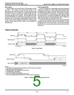
TIMING DIAGRAMS
1/fIN
1/fIN
t
SIH
tSIL
SHIFT IN
INPUT READY
INPUT DATA
t
IRH
t
IDH
tIRL
2747 drw 07
t
IDS
Figure 2. Input Timing
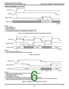
(7)
(2)
(4)
SHIFT IN
INPUT READY
INPUT DATA
(1)
(5)
(3)
(6)
STABLE DATA
2747 drw 08
NOTES:
1. Input Ready HIGH indicates space is available and a Shift In pulse may be applied.
2. Input Data is loaded into the first word.
3. Input Ready goes LOW indicating the first word is full.
4. The write pointer is incremented.
5. The FIFO is ready for the next word.
6. If the FIFO is full then the Input Ready remains LOW.
7. Shift In pulses applied while Input Ready is LOW will be ignored (see Figure 4).
Figure 3. The Mechanism of Shifting Data Into the FIFO
5.01
5

 IDT [ INTEGRATED DEVICE TECHNOLOGY ]