IDT72401, IDT72402, IDT72403, IDT72404
CMOS PARALLEL FIFO 64 x 4-BIT AND 64 x 5-BIT
MILITARY AND COMMERCIAL TEMPERATURE RANGES
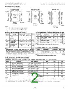
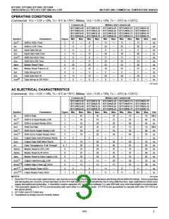
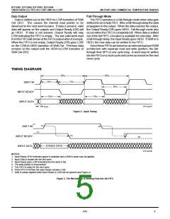
AC TEST CONDITIONS
Input Pulse Levels
5V
GND to 3.0V
Input Rise/Fall Times
Input Timing Reference Levels
Output Reference Levels
Output Load
3ns
1.5V
560
Ω
1.5V
OUTPUT
30pF*
See Figure 1
1.1K
Ω
2747 tbl 07
2747 drw 06
ALL INPUT PULSES:
or equivalent
circuit
3.0V
GND
90%
10%
90%
10%
Figure 1. AC Test Load
<3ns
<3ns
*Including scope and jig
2747 drw 05
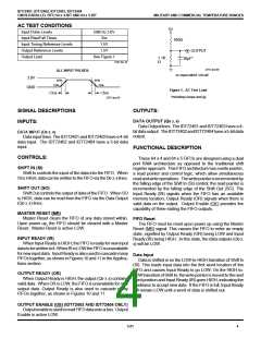
SIGNAL DESCRIPTIONS
OUTPUTS:
DATA OUTPUT (Q0-3, 4)
INPUTS:
Data Output lines. The IDT72401 and IDT72403 have a 4-
bitdataoutput. TheIDT72402andIDT72404havea5-bitdata
output.
DATA INPUT (D0-3, 4)
Data input lines. The IDT72401 and IDT72403 have a 4-bit
data input. The IDT72402 and IDT72404 have a 5-bit data
input.
FUNCTIONAL DESCRIPTION
CONTROLS:
These 64 x 4 and 64 x 5 FIFOs are designed using a dual
port RAM architecture as opposed to the traditional shift
register approach. This FIFO architecture has a write pointer,
a read pointer and control logic, which allow simultaneous
readandwriteoperations. Thewritepointerisincrementedby
the falling edge of the Shift In (Sl) control; the read pointer is
incremented by the falling edge of the Shift Out (SO). The
Input Ready (IR) signals when the FIFO has an available
memory location; Output Ready (OR) signals when there is
valid data on the output. Output Enable (OE) provides the
capability of three-stating the FIFO outputs.
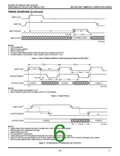
SHIFT IN (SI)
Shift In controls the input of the data into the FIFO. When
SI is HIGH, data can be written to the FIFO via the D0-3, 4 lines.
SHIFT OUT (SO)
Shift Out controls the output of data of the FIFO. When SO
is HIGH, data can be read from the FIFO via the Data Output
(Q0-3, 4) lines.
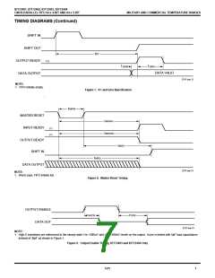
MASTER RESET (MR)
Master Reset clears the FIFO of any data stored within.
Upon power up, the FIFO should be cleared with a Master
Reset. Master Reset is active LOW.
FIFO Reset
The FIFO must be reset upon power up using the Master
Reset (MR) signal. This causes the FlFO to enter an empty
state, signified by Output Ready (OR) being LOW and Input
Ready (IR) being HIGH. In this state, the data outputs (Q0-3,
4) will be LOW.
INPUT READY (IR)
When Input Ready is HIGH, the FIFO is ready for new input
datatobewrittentoit.WhenIRisLOWtheFIFOisunavailable
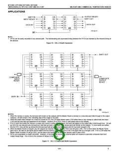
for new input data. Input Ready is also used to cascade many
FlFOs together, as shown in Figures 10 and 11 in the Applica-
tions section.
Data Input
Data is shifted in on the LOW-to-HlGH transition of Shift In
(Sl). This loads input data into the first word location of the
FIFO and causes Input Ready to go LOW. On the HlGH-to-
LOWtransitionofShiftIn,thewritepointerismovedtothenext
word position and Input Ready (IR) goes HIGH, indicating the
readiness to accept new data. If the FIFO is full, Input Ready
will remain LOW until a word of data is shifted out.
OUTPUT READY (OR)
When Output Ready is HIGH, the output (Q0-3, 4) contains
valid data. When OR is LOW, the FIFO is unavailable for new
output data. Output Ready is also used to cascade many
FlFOs together, as shown in Figures 10 and 11.
OUTPUT ENABLE (OE) (IDT72403 AND IDT72404 ONLY)
OutputenableisusedtoreadFIFOdataontoabus. Output
Enable is active LOW.
5.01
4

 IDT [ INTEGRATED DEVICE TECHNOLOGY ]