IDT72401, IDT72402, IDT72403, IDT72404
CMOS PARALLEL FIFO 64 x 4-BIT AND 64 x 5-BIT
MILITARY AND COMMERCIAL TEMPERATURE RANGES
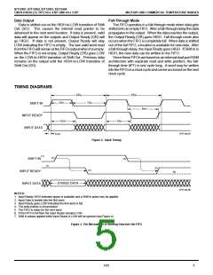
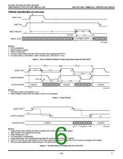
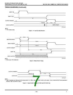
TIMING DIAGRAMS (Continued)
(2)
SHIFT OUT
(3)
(5)
SHIFT IN
(4)
tIPH
tPT
INPUT READY
INPUT DATA
(1)
tSIR
tHIR
STABLE DATA
2747 drw 09
NOTES:
1. FIFO is initially full.
2. Shift Out pulse is applied.
3. Shift In is held HIGH.
4. As soon as Input Ready becomes HIGH the Input Data is loaded into the FIFO.
5. The write pointer is incremented. Shift In should not go LOW until (tPT + tIPH).
Figure 4. Data is Shifted In Whenever Shift In and Input Ready are Both HIGH
1/fOUT
1/fOUT
tSOH
tSOL
tODS
(2)
SHIFT OUT
OUTPUT READY
OUTPUT DATA
tORH
tODH
tORL
A-DATA
B-DATA
C-DATA
(1)
2747 drw 10
NOTES:
1. This data is loaded consecutively A, B, C.
2. Data is shifted out when Shift Out makes a HIGH to LOW transition.
Figure 5. Output TIming
SHIFT OUT(7)
OUTPUT READY
OUTPUT DATA
(2)
(4)
(1)
(5)
(3)
(6)
A-DATA
B-DATA
2747 drw 11
A or B
NOTES:
1. Output Ready HIGH indicates that data is available and a Shift Out pulse may be applied.
2. Shift Out goes HIGH causing the next step.
3. Output Ready goes LOW.
4. The read pointer is incremented.
5. Output Ready goes HIGH indicating that new data (B) is now available at the FIFO outputs.
6. If the FIFO has only one word loaded (A DATA) then Output Ready stays LOW and the A DATA remains unchanged at the outputs.
7. Shift Out pulses applied when Output Ready is LOW will be ignored.
Figure 6. The Mechanism of Shifting Data Out of the FIFO
5.01
6

 IDT [ INTEGRATED DEVICE TECHNOLOGY ]