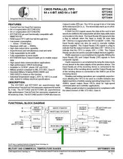
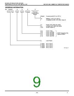
IDT72401, IDT72402, IDT72403, IDT72404
CMOS PARALLEL FIFO 64 x 4-BIT AND 64 x 5-BIT
MILITARY AND COMMERCIAL TEMPERATURE RANGES
OPERATING CONDITIONS
(Commercial: VCC = 5.0V ± 10%, TA = 0°C to +70°C; Military: VCC = 5.0V ± 10%, TA = –55°C to +125°C)
Commercial
Military and Commercial
IDT72401L45 IDT72401L35 IDT72401L25 IDT72401L15 IDT72401L10
IDT72402L45 IDT72402L35 IDT72402L25 IDT72402L15 IDT72402L10
IDT72403L45 IDT72403L35 IDT72403L25 IDT72403L15 IDT72403L10
IDT72404L45 IDT72404L35 IDT72404L25 IDT72404L15 IDT72404L10
Symbol
Parameters
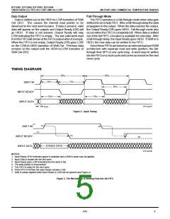
Shift in HIGH Time
FIgure Min.
Max.
—
Min.
9
Max.
—
Min.
11
24
0
Max.
—
Min.
11
25
0
Max.
—
Min.
11
30
0
Max. Unit
(1)
tSIH
2
2
2
2
5
5
8
8
4
4
7
9
11
0
—
—
—
—
—
—
—
—
—
—
—
ns
ns
tSIL
tIDS
tIDH
Shift in LOW TIme
—
17
0
—
—
—
Input Data Set-up
—
—
—
—
ns
Input Data Hold Time
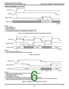
Shift Out HIGH Time
Shift Out LOW Time
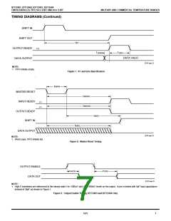
Master Reset Pulse
Master Reset Pulse to SI
Data Set-up to IR
13
9
—
15
9
—
20
11
24
25
10
5
—
30
11
25
25
25
5
—
40
11
25
30
35
5
ns
(1)
tSOH
—
—
—
—
ns
tSOL
tMRW
tMRS
tSIR
11
20
10
3
—
17
25
10
3
—
—
—
ns
—
—
—
—
ns
—
—
—
—
ns
—
—
—
—
ns
tHIR
Data Hold from IR
13
0
—
15
0
—
20
0
—
30
0
—
30
0
ns
(4)
tSOR
Data Set-up to OR HIGH
—
—
—
—
ns
2747 tbl 05
AC ELECTRICAL CHARACTERISTICS
(Commercial: VCC = 5.0V ± 10%, TA = 0°C to +70°C; Military: VCC = 5.0V ± 10%, TA = –55°C to +125°C)
Commercial
Military and Commercial
IDT72401L45 IDT72401L35 IDT72401L25 IDT72401L15 IDT72401L10
IDT72402L45 IDT72402L35 IDT72402L25 IDT72402L15 IDT72402L10
IDT72403L45 IDT72403L35 IDT72403L25 IDT72403L15 IDT72403L10
IDT72404L45 IDT72404L35 IDT72404L25 IDT72404L15 IDT72404L10
Symbol
Parameters
FIgure Min.
Max.
45
18
18
45
18
19
—
Min.
—
—
—
—
—
—
5
Max.
35
18
20
35
18
20
—
Min.
—
—
—
—
—
—
5
Max.
25
21
28
25
19
34
—
Min.
—
—
—
—
—
—
5
Max.
15
35
40
15
35
40
—
Min.
—
—
—
—
—
—
5
Max. Unit
tIN
Shift In Rate
2
2
—
—
—
—
—
—
5
10
40
45
10
40
55
—
MHz
ns
(1)
tIRL
Shift In to Input Ready LOW
Shift In to Input Ready HIGH
Shift Out Rate
(1)
tIRH
2
ns
tOUT
5
MHz
ns
(1)
tORL
Shift Out to Output Ready LOW
Shift Out to Output Ready HIGH
Output Data Hold (Previous Word)
Output Data Shift (Next Word)
Data Throughput or "Fall-Through"
Master Reset to OR LOW
5
(1)
tORH
5
ns
tODH
5
ns
tODS
5
—
—
—
—
19
30
25
25
—
—
—
—
20
34
28
28
—
—
—
—
34
40
35
35
—
—
—
—
40
65
35
35
—
—
—
—
55
65
40
40
ns
tPT
4, 7
8
ns
tMRORL
tMRIRH
ns
Master Reset to IR HIGH
8
ns
tMRQ
Master Reset to Data Output LOW
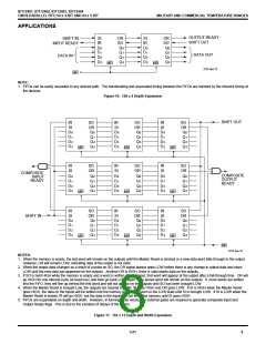
Output Valid from OE LOW
Output High-Z from OE HIGH
Input Ready Pulse HIGH
8
9
9
4
7
—
—
—
9
20
12
12
—
—
—
—
—
9
20
15
12
—
—
—
—
—
11
11
25
20
15
—
—
—
—
—
11
11
35
30
25
—
—
—
—
—
11
11
40
35
30
—
—
ns
ns
(3)
tOOE
(3,4)
tHZOE
ns
(2,4)
tIPH
ns
(2,4)
tOPH
Ouput Ready Pulse HIGH
9
9
ns
NOTES:
2747 tbl 06
1. Since the FIFO is a very high-speed device, care must be excercised in the design of the hardware and timing utilized within the design. Device grounding
and decoupling are crucial to correct operation as the FIFO will respond to very small glitches due to long reflective lines, high capacitances and/or poor
supply decoupling and grounding. A monolithic ceramic capacitor of 0.1µF directly between VCC and GND with very short lead length is recommended.
2. This parameter applies to FIFOs communicating with each other in a cascaded mode. IDT FIFOs are guaranteed to cascade with other IDT FIFOs of
like speed grades.
3. IDT72403 and IDT72404 only.
4. Guaranteed by design but not currently tested.
5.01
3

 IDT [ INTEGRATED DEVICE TECHNOLOGY ]