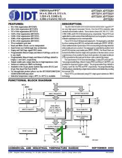
IDT72421/72201/72211/72221/72231/72241/72251 CMOS SyncFIFO™
64 x 9, 256 x 9, 512 x 9, 1,024 x 9, 2,048 x 9, 4,096 x 9 and 8,192 x 9
COMMERCIALANDINDUSTRIAL
TEMPERATURERANGES
ACELECTRICALCHARACTERISTICS
(Commercial: VCC = 5V ± 10%, TA = 0°C to +70°C; Industrial: VCC = 5V ± 10%, TA = –40°C to +85°C)
Commercial
IDT72421L10
IDT72201L10
IDT72211L10
IDT72221L10
IDT72231L10
IDT72241L10
IDT72251L10
Com'l & Ind'l(1)
Com'l & Ind'l(1)
IDT72421L25
IDT72201L25
IDT72211L25
IDT72221L25
IDT72231L25
IDT72241L25
IDT72251L25
IDT72421L15
IDT72201L15
IDT72211L15
IDT72221L15
IDT72231L15
IDT72241L15
IDT72251L15
Symbol
fS
Parameter
Clock Cycle Frequency
Min.
—
Max.
Min.
—
Max.
Min.
—
Max.
40
Unit
MHz
100
6.5
—
—
—
—
—
—
—
—
—
—
10
—
6
66.7
10
—
—
—
—
—
—
—
—
—
—
15
—
8
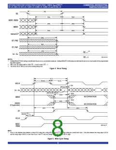
tA
DataAccessTime
ClockCycleTime
ClockHighTime
2
10
4.5
4.5
3
2
15
6
2
25
10
10
6
15
—
—
—
—
—
—
—
—
—
—
25
—
13
13
15
15
15
15
—
ns
ns
ns
ns
ns
ns
ns
ns
ns
ns
ns
ns
ns
ns
ns
ns
ns
ns
ns
ns
tCLK
tCLKH
tCLKL
tDS
ClockLowTime
6
DataSetupTime
4
tDH
DataHoldTime
0.5
3
1
1
tENS
tENH
tRS
EnableSetupTime
EnableHoldTime
ResetPulseWidth(2)
ResetSetupTime
Reset Recovery Time
ResettoFlagandOutputTime
4
6
0.5
10
8
1
1
15
10
10
—
0
15
15
15
—
0
tRSS
tRSR
tRSF
tOLZ
tOE
8
—
0
(3)
OutputEnabletoOutputinLow-Z
OutputEnabletoOutputValid
3
3
3
(3)
tOHZ
tWFF
tREF
tPAF
tPAE
tSKEW1
OutputEnabletoOutputinHigh-Z
WriteClocktoFullFlag
3
6
3
8
3
—
—
—
—
5
6.5
6.5
6.5
6.5
—
—
—
—
—
6
10
10
10
10
—
—
—
—
—
10
ReadClocktoEmptyFlag
WriteClocktoProgrammableAlmost-FullFlag
ReadClocktoProgrammableAlmost-EmptyFlag
SkewtimebetweenReadClock& WriteClockfor
Empty Flag & Full Flag
tSKEW2
SkewtimebetweenReadClock&WriteClockfor
Almost-EmptyFlag&ProgrammableAlmost-FullFlag
14
—
15
—
18
—
ns
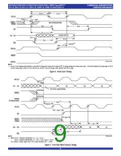
NOTES:
1. Industrial temperature range product for the 15ns and 25ns speed grades are available as standard product.
2. Pulse widths less than minimum values are not allowed.
3. Values guaranteed by design, not currently tested.
5V
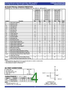
ACTESTCONDITIONS
In Pulse Levels
GND to 3.0V
3ns
1.5V
1.5V
See Figure 1
1.1K
Input Rise/Fall Times
Input Timing Reference Levels
Output Reference Levels
Output Load
D.U.T.
30pF*
680Ω
CAPACITANCE(Ta = +25°C, f = 1.0MHz)
Symbol
Parameter
InputCapacitance
OutputCapacitance
Conditions
Max. Unit
2655 drw 03
(2)
CIN
VIN = 0V
10
10
pF
pF
(1,2)
COUT
NOTES:
VOUT = 0V
or equivalent circuit
Figure 1. Output Load
*includesjigandscopecapacitances
1. With output deselected (OE ≥ VIH).
2. Characterized values, not currently tested.
4

 IDT [ INTEGRATED DEVICE TECHNOLOGY ]