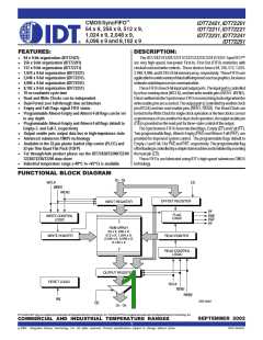
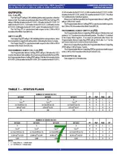
IDT72421/72201/72211/72221/72231/72241/72251 CMOS SyncFIFO™
64 x 9, 256 x 9, 512 x 9, 1,024 x 9, 2,048 x 9, 4,096 x 9 and 8,192 x 9
COMMERCIALANDINDUSTRIAL
TEMPERATURERANGES
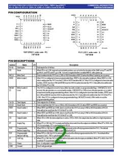
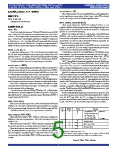
PINCONFIGURATION
INDEX
INDEX
4
3
2
32 31 30
1
29 28 27 26 25
32 31 30
D1
29
28
27
26
25
24
23
22
21
RS
5
1
2
3
4
D
1
24
23
22
21
20
19
18
17
D
0
WEN1
WEN1
WCLK
WEN2/LD
6
D0
WCLK
PAF
PAE
7
PAF
WEN2/LD
8
PAE
GND
VCC
9
VCC
GND
REN1
RCLK
REN2
OE
5
Q8
Q8
10
11
12
13
REN1
Q7
6
7
8
Q7
RCLK
Q6
Q6
REN2
Q5
Q5
9
10 11 12 13 14 15 16
14 15 16 17 18 19 20
2655 drw 02
2655 drw02a
TQFP (PR32-1, order code: PF)
TOP VIEW
PLCC (J32-1, order code: J)
TOP VIEW
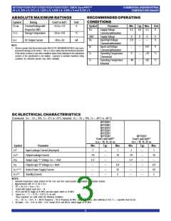
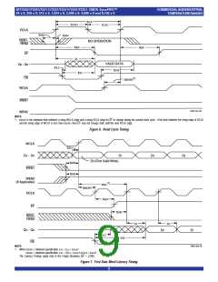
PINDESCRIPTIONS
Symbol
D0-D8
RS
Name
DataInputs
I/O
Description
I
I
Datainputs fora9-bitbus.
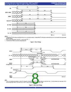
Reset
WhenRS is set LOW, internal read and write pointers are set to the first location of the RAM array,FF andPAF
go HIGH, and PAE and EF go LOW. A reset is required before an initial WRITE after power-up.
WCLK
WriteClock
I
I
DataiswrittenintotheFIFOonaLOW-to-HIGHtransitionofWCLKwhentheWriteEnable(s)areasserted.
WEN1
WriteEnable1
Ifthe FIFOis configuredtohave programmable flags, WEN1 is the onlywrite enable pin. WhenWEN1 is LOW,
data is writtenintothe FIFOoneveryLOW-to-HIGHtransitionWCLK. Ifthe FIFOis configuredtohave twowrite
enables, WEN1 mustbeLOWandWEN2mustbeHIGHtowritedataintotheFIFO.Datawillnotbewritteninto
the FIFOifthe FF is LOW.
WEN2/ WriteEnable2/
I
The FIFO is configured at reset to have either two write enables or programmable flags. If WEN2/LD is HIGH
atreset,this pinoperates as asecondwriteenable. IfWEN2/LD is LOWatreset,this pinoperates as acontrol
toloadandreadtheprogrammableflagoffsets.IftheFIFOis configuredtohavetwowriteenables,WEN1 must
be LOWandWEN2mustbe HIGHtowrite data intothe FIFO. Data willnotbe writtenintothe FIFOifthe FF is
LOW. Ifthe FIFOis configuredtohave programmable flags, WEN2/LD is heldLOWtowrite orreadthe
programmableflagoffsets.
LD
Load
Q0-Q8
RCLK
REN1
DataOutputs
ReadClock
O Dataoutputsfora9-bitbus.
I
I
Data is read from the FIFO on a LOW-to-HIGH transition of RCLK when REN1 and REN2 are asserted.
WhenREN1 and REN2 are LOW, data is read from the FIFO on every LOW-to-HIGH transition of RCLK.
Data will not be read from the FIFO if the EF is LOW.
Read Enable 1
REN2
OE
Read Enable 2
OutputEnable
EmptyFlag
I
I
WhenREN1 and REN2 are LOW, data is read from the FIFO on every LOW-to-HIGH transition of RCLK.
Data will not be read from the FIFO if the EF is LOW.
When OE is LOW, the data outputbus is active. IfOE is HIGH, the outputdata bus willbe ina high-impedance
state.
EF
O WhenEF is LOW, the FIFOis emptyandfurtherdata reads fromthe outputare inhibited. WhenEF is HIGH, the
FIFO is not empty. EF is synchronized to RCLK.
PAE
PAF
FF
Programmable
Almost-EmptyFlag
O WhenPAE isLOW,theFIFOisalmost-emptybasedontheoffsetprogrammedintotheFIFO.Thedefault
offsetatresetis Empty+7.PAE is synchronizedtoRCLK.
O WhenPAFisLOW,theFIFOisalmost-fullbasedontheoffsetprogrammedintotheFIFO.Thedefaultoffset
at reset is Full-7. PAF is synchronized to WCLK.
O WhenFF is LOW, the FIFOis fullandfurtherdata writes intothe inputare inhibited. When FF is HIGH, the FIFO
isnotfull.FF issynchronizedtoWCLK.
Programmable
Almost-FullFlag
Full Flag
VCC
Power
One +5 volt power supply pin.
One 0 volt ground pin.
GND
Ground
2

 IDT [ INTEGRATED DEVICE TECHNOLOGY ]