IDT72421/72201/72211/72221/72231/72241/72251 CMOS SyncFIFO™
64 x 9, 256 x 9, 512 x 9, 1,024 x 9, 2,048 x 9, 4,096 x 9 and 8,192 x 9
COMMERCIALANDINDUSTRIAL
TEMPERATURERANGES
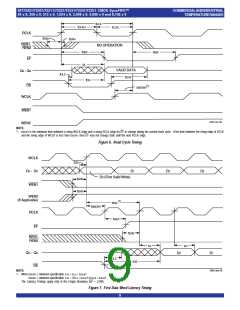
tCLK
tCLKH
tCLKL
RCLK
tENS
tENH
REN1,
REN2
NO OPERATION
tREF
tREF
EF
tA
VALID DATA
Q0 - Q8
tOLZ
tOHZ
tOE
OE
(1)
SKEW1
t
WCLK
WEN1
2655 drw 08
WEN2
NOTE:
1. tSKEW1 is the minimum time between a rising WCLK edge and a rising RCLK edge for EF to change during the current clock cycle. If the time between the rising edge of RCLK
and the rising edge of WCLK is less than tSKEW1, then EF may not change state until the next RCLK edge.
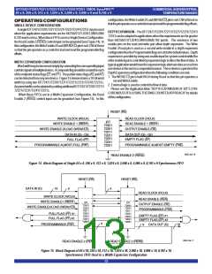
Figure 6. Read Cycle Timing
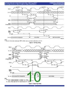
WCLK
tDS
D0
- D8
D1
D2
D3
D0
(First Valid Write)
tENS
WEN1
tENS
WEN2
(If Applicable)
(1)
tFRL
tSKEW1
RCLK
tREF
EF
tENS
REN1,
REN2
tA
tA
Q0 - Q8
D0
D1
tOLZ
tOE
OE
2655 drw 09
NOTE:
1. When tSKEW1 ≥ minimum specification, tFRL = tCLK + tSKEW1
When tSKEW1 < minimum specification, tFRL = 2tCLK + tSKEW1 or tCLK + tSKEW1
The Latency Timings apply only at the Empty Boundary (EF = LOW).
Figure 7. First Data Word Latency Timing
9

 IDT [ INTEGRATED DEVICE TECHNOLOGY ]