IDT72421/72201/72211/72221/72231/72241/72251 CMOS SyncFIFO™
64 x 9, 256 x 9, 512 x 9, 1,024 x 9, 2,048 x 9, 4,096 x 9 and 8,192 x 9
COMMERCIALANDINDUSTRIAL
TEMPERATURERANGES
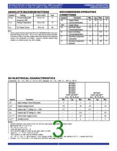
ABSOLUTEMAXIMUMRATINGS
RECOMMENDEDOPERATING
CONDITIONS
Symbol
Rating
Com'l & Ind'l
Unit
Symbol
Parameter
Min. Typ. Max.
Unit
VTERM
TerminalVoltagewith
RespecttoGND
StorageTemperature
–0.5to+7.0
V
VCC
SupplyVoltage
Commercial/Industrial
SupplyVoltage
InputHighVoltage
Commercial/Industrial
InputLowVoltage
Commercial/Industrial
OperatingTemperature
Commercial
4.5
5.0
5.5
V
TSTG
–55to +125
–50 to +50
°C
GND
VIH
0
0
0
V
V
2.0
—
—
IOUT
DCOutputCurrent
mA
NOTE:
VIL
TA
TA
—
0
—
—
—
0.8
+70
+85
V
°C
°C
1. Stresses greater than those listed under ABSOLUTE MAXIMUM RATINGS may cause
permanent damage to the device. This is a stress rating only and functional operation
of the device at these or any other conditions above those indicated in the operational
sections of the specification is not implied. Exposure to absolute maximum rating
conditions for extended periods may affect reliability.
OperatingTemperature
Industrial
–40
DCELECTRICALCHARACTERISTICS
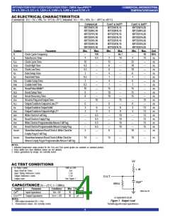
(Commercial: VCC = 5V ± 10%, T
A
= 0°
C to +70
°
C; Industrial: VCC = 5V ± 10%, T
A
= –40
°
C to +85
°
C)
IDT72421
IDT72201
IDT72211
IDT72221
IDT72231
IDT72241
IDT72251
Com'l and Ind'l(1)
CLK = 10, 15, 25 ns
Com'l and Ind'l(1)
tCLK = 10, 15, 25 ns
t
Symbol
Parameter
Min.
–1
Typ.
—
—
—
—
—
—
Max.
1
Min.
–1
Typ.
—
—
—
—
—
—
Max.
(2)
ILI
Input Leakage Current (Any Input)
OutputLeakageCurrent
1
10
—
0.4
50
5
(3)
ILO
–10
2.4
—
10
—
0.4
35
5
–10
2.4
—
VOH
VOL
Output Logic “1” Voltage, IOH = –2mA
OutputLogic“0”Voltage,IOL=8mA
Active Power Supply Current
StandbyCurrent
(4,5,6)
ICC1
—
—
(4,7)
ICC2
—
—
NOTES:
1. Industrial temperature range product for the 15ns and 25ns speed grades are available as standard product.
2. Measurements with 0.4 ≤ VIN ≤ VCC.
3. OE ≥ VIH, 0.4 ≤ VOUT ≤ VCC.
4. Tested with outputs open (IOUT = 0).
5. RCLK and WCLK toggle at 20 MHz and data inputs switch at 10 MHz.
6. Typical ICC1 = 1.7 + 0.7*fS + 0.02*CL*fS (in mA).
These equations are valid under the following conditions:
VCC = 5V, TA = 25°C, fS = WCLK frequency = RCLK frequency (in MHz, using TTL levels), data switching at fS/2, CL = capacitive load (in pF).
7. All Inputs = VCC - 0.2V or GND + 0.2V, except RCLK and WCLK, which toggle at 20 MHz.
3

 IDT [ INTEGRATED DEVICE TECHNOLOGY ]