IDT72421/72201/72211/72221/72231/72241/72251 CMOS SyncFIFO™
64 x 9, 256 x 9, 512 x 9, 1,024 x 9, 2,048 x 9, 4,096 x 9 and 8,192 x 9
COMMERCIALANDINDUSTRIAL
TEMPERATURERANGES
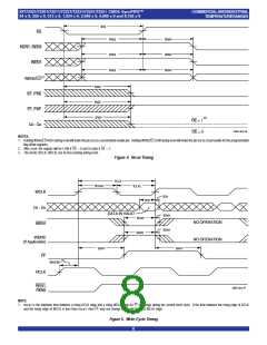
tRS
RS
REN1, REN2
WEN1
tRSS
tRSS
tRSS
tRSR
tRSR
tRSR
WEN2/LD(1)
EF, PAE
tRSF
tRSF
FF, PAF
tRSF
OE = 1(2)
Q0 - Q8
2655 drw 06
OE = 0
NOTES:
1. Holding WEN2/LD HIGH during reset will make the pin act as a second write enable pin. Holding WEN2/LD LOW during reset will make the pin act as a load enable for the programmable
flag offset registers.
2. After reset, the outputs will be LOW if OE = 0 and tri-state if OE = 1.
3. The clocks (RCLK, WCLK) can be free-running during reset.
Figure 4. Reset Timing
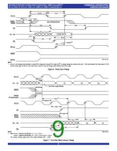
tCLK
tCLKH
tCLKL
WCLK
tDH
tDS
D0 - D8
DATA IN VALID
t
ENH
ENH
t
ENS
NO OPERATION
NO OPERATION
WEN1
t
tENS
WEN2/
(If Applicable)
t
WFF
tWFF
FF
(1)
tSKEW1
RCLK
REN1,
REN2
2655 drw 07
NOTE:
1. tSKEW1 is the minimum time between a rising RCLK edge and a rising WCLK edge for FF to change during the current clock cycle. If the time between the rising edge of RCLK
and the rising edge of WCLK is less than tSKEW1, then FF may not change state until the next WCLK edge.
Figure 5. Write Cycle Timing
8

 IDT [ INTEGRATED DEVICE TECHNOLOGY ]