IDT70825S/L
High-Speed 8K x 16 Sequential Access Random Access Memory
Industrial and Commercial Temperature Ranges
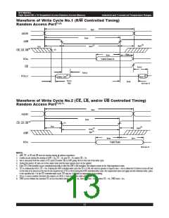
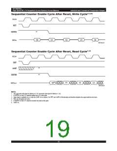
Sequential Counter Enable Cycle After Reset, Write Cycle(1,4,6)
SCLK
RST
(2)
CNTEN
D0
D1
D2
D3
D4
SI/OIN
3016 drw 23
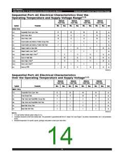
Sequential Counter Enable Cycle After Reset, Read Cycle(1,4)
SCLK
RST
(3)
SR/W
(5)
CNTEN
D0(5)
D3
D1
D2
SI/OOUT
3016 drw 24
NOTES:
1. 'D0' represents data input for Address=0, 'D1' represents data input for Address=1, etc.
1. If CNTEN=VIL then 'D1' would be written into 'A1' at this point.
3. Data output is available at a tCD after the SR/W=VIH is clocked. The RST sets SR/W=LOW internally and therefore disables the output until the next clock.
4. SCE=VIL throughout all cycles.
5. If CNTEN=VIL then 'D1' would be clocked out (read) at this point.
6. SR/W=VIL.
6.42
19

 IDT [ INTEGRATED DEVICE TECHNOLOGY ]