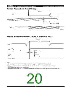
IDT70825S/L
High-Speed 8K x 16 Sequential Access Random Access Memory
Industrial and Commercial Temperature Ranges
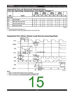
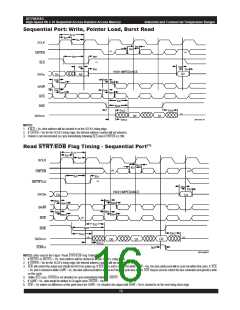
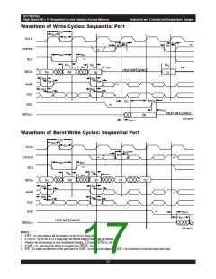
Sequential Port: Write, Pointer Load, Burst Read
tCYC
tCH
tCL
SCLK
CNTEN
SLD
tEH
tES
(3)
(2)
t
EH
(1)
t
ES
t
DS
t
DS
tDH
tDH
HIGH IMPEDANCE
D2
SI/OIN
Dx
A0
tWS
t
WS
tWH
t
WH
SR/W
SCE
t
WS
tWS
tWH
tWH
tCD
tSOE
SOE
t
OLZ
tOHZ
(2)
SI/OOUT
D0
D1
3016 drw 18
t
CKLZ
NOTES:
1. If SLD = VIL, then address will be clocked in on the SCLK's rising edge.
2. If CNTEN = VIH for the SCLK's rising edge, the internal address counter will not advance.
3. Pointer is not incremented on cycle immediately following SLD even if CNTEN is LOW.
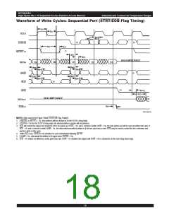
Read STRT/EOB Flag Timing - Sequential Port(1)
tCYC
tCH
tCL
SCLK
CNTEN
tEH
tES
(4)
(2)
tES
tEH
(1)
SSTRT1/2
t
DS
tDH
HIGH IMPEDANCE
SI/OIN
Dx
D3
tWS
tWS
tWH
t
WH
SR/W
SCE
SOE
tWS
tWS
tWH
t
WH
(3)
t
CD
t
SOE
t
OHZ
tOLZ
(5)
(2)
SI/OOUT
D2
D0
D1
tCKLZ
EOB1/2
tEB
3016 drw19
NOTES: (Also used in the Figure "Read STRT/EOB Flag Timing")
1. If SSTRT1 or SSTRT2 = VIL, then address will be clocked in on the SCLK's rising edge.
2. If CNTEN = VIH for the SCLK's rising edge, the internal address counter will not advance.
3. SOE will control the output and should be HIGH on power-up. If SCE = VIL and is clocked in while SR/W = VIH, the data addressed will be read out within that cycle. If SCE
= VIL and is clocked in while SR/W = VIL, the data addressed will be written to if the last cycle was a read. SOE may be used to control the bus contention and permit a write
on this cycle.
4. Unlike SLD case, CNTEN is not disabled on cycle immediately following SSTRT.
5. If SR/W = VIL, data would be written to D0 again since CNTEN = VIH.
6. SOE = VIL makes no difference at this point since the SR/W = VIL disables the output until SR/W = VIH is clocked in on the next rising clock edge.
16

 IDT [ INTEGRATED DEVICE TECHNOLOGY ]