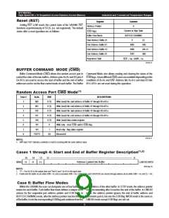
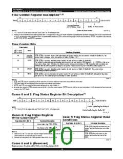
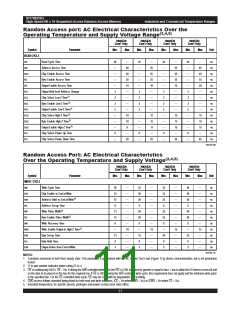
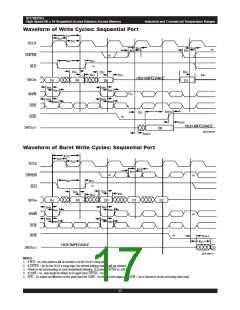
IDT70825S/L
High-Speed 8K x 16 Sequential Access Random Access Memory
Industrial and Commercial Temperature Ranges
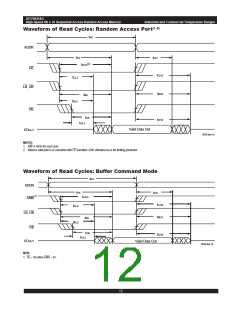
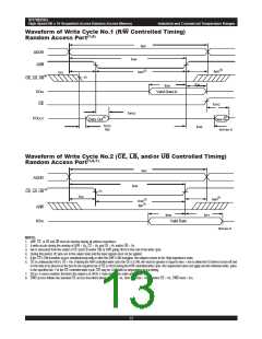
Waveform of Write Cycle No.1 (R/W Controlled Timing)
Random Access Port(1,6)
tWC
ADDR
R/W
tAW
(3)
(2)
WP
tWR
t
tAS
CE, LB, UB(8)
(5)
tDH
tDW
I/OIN
Valid Data In
OE
tOHZ
tWHZ
(4)
Data Out
Data Out(4)
I/OOUT
t
ACS
tOW
3016 drw 15
tBE
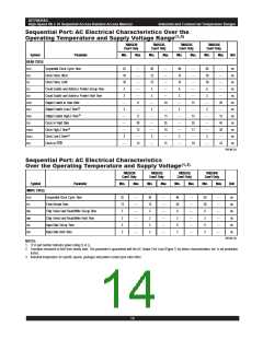
Waveform of Write Cycle No.2 (CE, LB, and/or UB Controlled Timing)
Random Access Port(1,6,7)
t
WC
ADDR
t
AW
CE, LB, UB (8)
(5)
tAS
(3)
WR
(2)
t
t
t
CW
(2)
BP
R/W
t
DW
tDH
I/OIN
Valid Data
3016 drw 16
NOTES:
1. R/W, CE, or LB and UB must be inactive during all address transitions.
2. A write occurs during the overlap of R/W = VIL, CE = VIL and LB = VIL and/or UB = VIL.
3. tWR is measured from the earlier of CE (and LB and/or UB) or R/W going HIGH to the end of the write cycle.
4. During this period, I/O pins are in the output state and the input signals must not be applied.
5. If the CE LOW transition occurs simultaneously with or after the R/W LOW transition, the outputs remain in the High-impedance state.
6. OE is continuously HIGH, OE = VIH. If during the R/W controlled write cycle the OE is LOW, tWP must be greater or equal to tWHZ + tDW to allow the I/O drivers to turn off and
on the data to be placed on the bus for the required tDW. If OE is HIGH during the R/W controlled write cycle, this requirement does not apply and the minimum write pulse
is the specified tWP. For the CE controlled write cycle, OE may be LOW with no degregation to tCW timing.
7. I/OOUT is never enabled, therefore the output is in HIGH-Z state during the entire write cycle.
8. CMD access follows the standard CE access described above. If CMD = VIL, then CE must = VIH or, when CE = VIL, CMD must = VIH.
6.42
13

 IDT [ INTEGRATED DEVICE TECHNOLOGY ]