IC42S16100
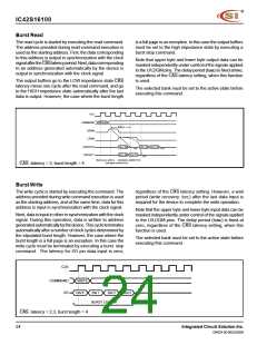
Burst Read
The read cycle is started by executing the read command.
The address provided during read command execution is
used as the starting address. First, the data corresponding
to this address is output in synchronization with the clock
signal after theCASlatency period. Next, data corresponding
to an address generated automatically by the device is
output in synchronization with the clock signal.
is a full page is an exception. In this case the output buffers
must be set to the high impedance state by executing a
burst stop command.
Note that upper byte and lower byte output data can be
masked independently under control of the signals applied
to the U/LDQM pins. The delay period (tQMD) is fixed at two,
regardless of the CAS latency setting, when this function
is used.
The output buffers go to the LOW impedance state CAS
latency minus one cycle after the read command, and go
to the HIGH impedance state automatically after the last
data is output. However, the case where the burst length
The selected bank must be set to the active state before
executing this command.
CLK
COMMAND
UDQM
READ A0
t
QMD=2
LDQM
I/O8-I/O15
I/O0-I/O 7
D
OUT A0
D
OUT A2
DOUT A3
HI-Z
HI-Z
DOUT A0
D
OUT A1
HI-Z
READ (CA=A, BANK 0)
DATA MASK (LOWER BYTE)
DATA MASK (UPPER BYTE)
CAS latency = 2, burst length = 4
Burst Write
The write cycle is started by executing the command. The
address provided during write command execution is used
as the starting address, and at the same time, data for this
address is input in synchronization with the clock signal.
regardless of the CAS latency setting. However, a wait
period (write recovery: tDPL) after the last data input is
required for the device to complete the write operation.
Note that the upper byte and lower byte input data can be
masked independently under control of the signals applied
to the U/LDQM pins. The delay period (tDMD) is fixed at
zero, regardless of the CAS latency setting, when this
function is used.
Next, data is input in other in synchronization with the clock
signal. During this operation, data is written to address
generatedautomaticallybythedevice. Thiscycleterminates
automatically after a number of clock cycles determined by
the stipulated burst length. However, the case where the
burst length is a full page is an exception. In this case the
write cycle must be terminated by executing a burst stop
command. The latency for I/O pin data input is zero,
The selected bank must be set to the active state before
executing this command.
CLK
COMMAND
I/O
WRITE
DIN
0
DIN
1
DIN
2
DIN 3
BURST LENGTH
CAS latency = 2,3, burst length = 4
24
Integrated Circuit Solution Inc.
DR024-0D 06/25/2004

 ICSI [ INTEGRATED CIRCUIT SOLUTION INC ]