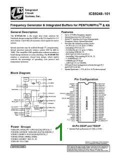
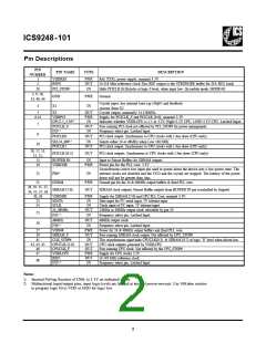
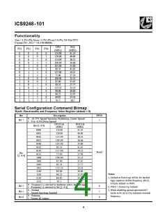
ICS9248-101
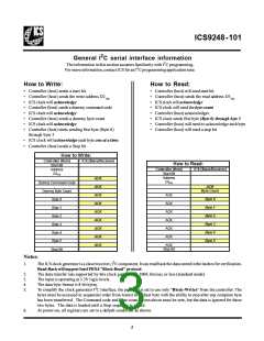
General I2C serial interface information
The information in this section assumes familiarity with I2C programming.
For more information, contact ICS for an I2C programming application note.
How to Write:
Controller (host) sends a start bit.
Controller (host) sends the write address D2 (H)
ICS clock will acknowledge
How to Read:
Controller (host) will send start bit.
Controller (host) sends the read address D3 (H)
ICS clock will acknowledge
Controller (host) sends a dummy command code
ICS clock will acknowledge
ICS clock will send the byte count
Controller (host) acknowledges
Controller (host) sends a dummy byte count
ICS clock will acknowledge
Controller (host) starts sending first byte (Byte 0)
through byte 5
ICS clock sends first byte (Byte 0) through byte 5
Controller (host) will need to acknowledge each byte
Controller (host) will send a stop bit
ICS clock will acknowledge each byte one at a time.
Controller (host) sends a Stop bit
How to Write:
Controller (Host)
ICS (Slave/Receiver)
How to Read:
Start Bit
Controller (Host)
ICS (Slave/Receiver)
Address
Start Bit
D2(H)
Address
D3(H)
ACK
ACK
ACK
ACK
ACK
ACK
ACK
ACK
ACK
Dummy Command Code
ACK
Byte Count
Dummy Byte Count
Byte 0
ACK
ACK
ACK
ACK
ACK
ACK
Byte 0
Byte 1
Byte 2
Byte 3
Byte 4
Byte 5
Byte 1
Byte 2
Byte 3
Byte 4
Byte 5
ACK
Stop Bit
Stop Bit
Notes:
1.
The ICS clock generator is a slave/receiver, I2C component. It can read back the data stored in the latches for verification.
Read-BackwillsupportIntelPIIX4"Block-Read"protocol.
2.
3.
4.
5.
The data transfer rate supported by this clock generator is 100K bits/sec or less (standard mode)
The input is operating at 3.3V logic levels.
The data byte format is 8 bit bytes.
To simplify the clock generator I2C interface, the protocol is set to use only "Block-Writes" from the controller. The
bytes must be accessed in sequential order from lowest to highest byte with the ability to stop after any complete byte
has been transferred. The Command code and Byte count shown above must be sent, but the data is ignored for those
two bytes. The data is loaded until a Stop sequence is issued.
6.
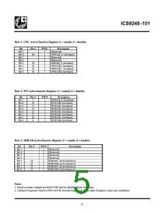
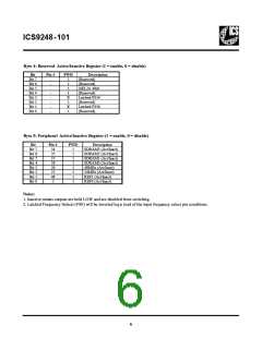
At power-on, all registers are set to a default condition, as shown.
3

 ICSI [ INTEGRATED CIRCUIT SOLUTION INC ]