ICS9248-101
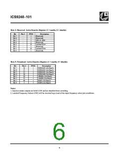
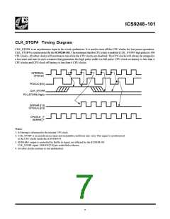
CLK_STOP# Timing Diagram
CLK_STOP# is an asychronous input to the clock synthesizer. It is used to turn off the CPU clocks for low power operation.
CLK_STOP# is synchronized by the ICS9248-101. The minimum that the CPU clock is enabled (CLK_STOP# high pulse) is 100
CPU clocks. All other clocks will continue to run while the CPU clocks are disabled. The CPU clocks will always be stopped in
a low state and start in such a manner that guarantees the high pulse width is a full pulse. CPU clock on latency is less than 4
CPU clocks and CPU clock off latency is less than 4 CPU clocks.
INTERNAL
CPUCLK
PCICLK [6:0]
CLK_STOP#
PCI_STOP# (High)
SDRAM [7:0]
CPUCLK [2:0]
CPUCLK _F
SDRAM_F
Notes:
1. All timing is referenced to the internal CPU clock.
2. CLK_STOP# is an asynchronous input and metastable conditions may exist. This signal is synchronized
to the CPU clocks inside the ICS9248-101.
3. SDRAM-F output is controlled by Buffer in signal, not affected by the ICS9248-101
CLK_STOP# signal. SDRAM [7:0] are controlled as shown.
4. All other clocks continue to run undisturbed.
7

 ICSI [ INTEGRATED CIRCUIT SOLUTION INC ]