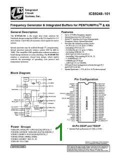
ICS9248-101
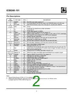
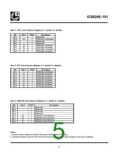
Pin Descriptions
PIN
PIN NAME
TYPE
DESCRIPTION
Ref, XTAL power supply, nominal 3.3V
NUMBER
1
2
VDDREF
REF0
PWR
OUT
14.318 Mhz reference clock.This REF output is the STRONGER buffer for ISA BUS loads
20
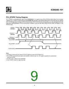
PCI_STOP#
IN
Halts PCICLK [6:0]clocks at logic 0 level, when input low (In mobile mode, MODE=0)
3, 9, 16,
33, 40, 44
GND
PWR
Ground
Crystal input, has internal load cap (36pF) and feedback
resistor from X2
4
X1
IN
5
6,14
X2
OUT
PWR
IN
Crystal output, nominally 14.318MHz.
VDDPCI
CPU2.5_3.3#1,2
PCICLK_F
FS31,2
Supply for PCICLK_F and PCICLK [6:0], nominal 3.3V
Indicates whether VDDLCPU is 2.5 or 3.3V. High=2.5V CPU, LOW=3.3V CPU. Latched Input.
Free running PCI clock not affected by PCI_STOP# for power management.
Frequency select pin. Latched Input.
7
8
OUT
IN
PCICLK0
OUT
PCI clock output. Synchronous to CPU clocks with 1-4ns skew (CPU early)
SEL24_48#1,2
PCICLK1
IN
OUT
Selects either 24 or 48MHz when Low =48 MHz
PCI clock output. Synchronous to CPU clocks with 1-4ns skew (CPU early)
10
18, 17, 13,
12, 11,
15
PCICLK [6:2]
OUT
PCI clock outputs. Synchronous to CPU clocks with 1-4ns skew (CPU early)
BUFFER IN
VDDCOR
IN
PWR
Input to Fanout Buffers for SDRAM outputs.
Power pin for the PLL core. 3.3V
19
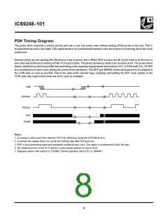
Asynchronous active low input pin used to power down the device into a low power state. The
internal clocks are disabled and the VCO and the crystal are stopped. The latency of the power
down will not be greater than 4ms.
21
PD#1
IN
22
28, 29, 31, 32,
34, 35, 37, 38
30, 36
GND48
PWR
OUT
Ground pin for the 24 & 48MHz output buffers & fixed PLL core.
SDRAM [7:0]
SDRAM clock outputs, Fanout Buffer outputs from BUFFER IN pin (controlled by chipset).
VDDSDR
SDATA
SCLK
PWR
IN
IN
Supply for SDRAM [7:0] and CPU PLL Core, nominal 3.3V.
Data input for I2C serial input, 5V tolerant input
Clock input of I2C input, 5V tolerant input
23
24
24_48MHz
OUT
24MHz or 48MHz output clock selectable by pin 10
25
26
FS11, 2
48MHz
FS01, 2
IN
OUT
IN
Frequency select pin. Latched Input.
48MHz output clock
Frequency select pin. Latched Input
27
VDD48
PWR
OUT
IN
OUT
OUT
PWR
OUT
IN
Power for 24 & 48MHz output buffers and fixed PLL core.
Free running SDRAM clock output. Not affected by CPU_STOP#
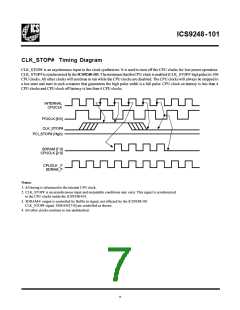
This asynchronous input halts CPUCLK(0:2), & SDRAM (0:7) at logic "0" level when driven low.
CPU clock outputs, powered by VDDLCPU
Free running CPU clock. Not affected by the CPU_STOP#
Supply for CPU clocks 2.5V
39
41
SDRAM_F
CLK_STOP#
CPUCLK [2:0]
CPUCLK_F
VDDLCPU
REF1
42, 43, 45
46
47
14.318 MHz reference clock.
48
FS21, 2
Frequency select pin. Latched Input
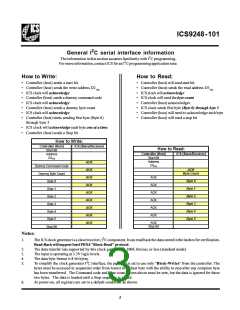
Notes:
1: Internal Pull-up Resistor of 120K to 3.3V on indicated inputs
2: Bidirectional input/output pins, input logic levels are latched at internal power-on-reset. Use 10Kohm resistor
to program logic Hi to VDD or GND for logic low.
2

 ICSI [ INTEGRATED CIRCUIT SOLUTION INC ]