iC-MR 13-BIT S&H SIN/COS
INTERPOLATOR WITH CONTROLLER INTERFACES
Rev A1, Page 29/44
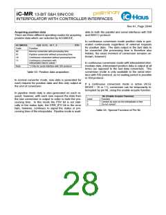
EEPROM INTERFACE
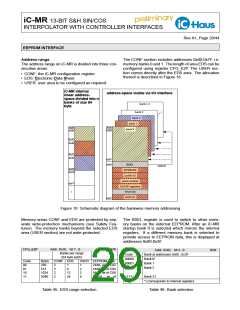
Address range
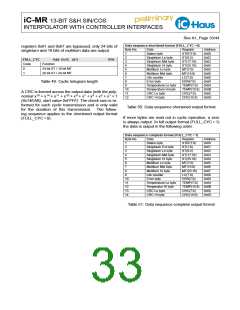
The CONF section includes addresses 0x00-0x7F, i.e.
The address range on iC-MR is divided into three con- memory banks 0 and 1. The length of area EDS can be
secutive areas:
configured using register CFG_E2P. The USER sec-
tion comes directly after the EDS area. The allocation
thereof is described in Figure 16.
• CONF: the iC-MR configuration register
• EDS: Electronic-Data-Sheet
• USER: user area to be configured as required.
iC-MR internal
linear address-
space divided into n
banks of size 64
byte
address-space visible via I/O interface
bank n-1
bank 3
bank 2
bank 1
bank 0
ADR
ADR
0x00
0x00
0x3F
0x40
0x7F
0x80
0x3F
0x40
BSEL
selects
0xBF
0xC0
EDSBANK
profile ID
serial number
0xFF
SLAVE-registers
STATUS
BiSS-ID
0x7F
Figure 16: Schematic diagram of the bankwise memory addressing
Memory areas CONF and EDS are protected by sep- The BSEL register is used to switch to other mem-
arate write-protection mechanisms (see Safety Fea- ory banks on the external EEPROM. After an iC-MR
tures). The memory banks beyond the selected EDS startup bank 0 is selected which mirrors the internal
area (USER section) are not write-protected.
registers. If a different memory bank is selected to
provide access to EEPROM data, this is displayed at
addresses 0x00-0x3F.
CFG_E2P
Addr. 0x26; bit 7...6
Banks per range
(64 byte each)
R/W
BSEL
Code
00000
00001
00010
...
Addr. 0x40; bit 4...0
R/W
Bank at addresses 0x00...0x3F
Bank 0*
Code
00
01
10
11
Bytes
256
512
1024
2048
CONF EDS
USER EEPROM, Type
Bank 1
2
2
2
2
1
4
12
24
1
2
2
6
2 kbit, as of C02
4 kbit, as of C04
8 kbit, as of C08
16 kbit, as of
C016
Bank 2
...
11111
Note
Bank 31
*) Corresponds to internal registers
Table 45: EDS range selection
Table 46: Bank selection

 ICHAUS [ IC-HAUS GMBH ]