IBM3009K2672
IBM SONET/SDH Framer
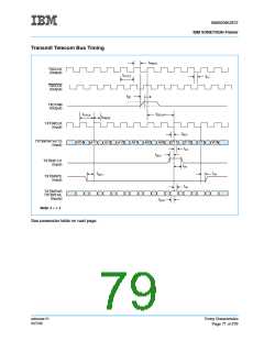
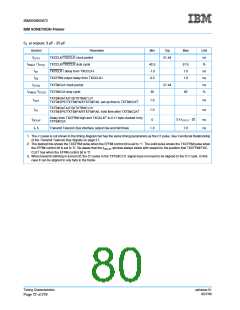
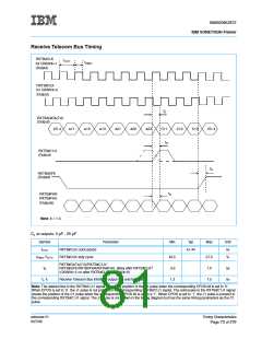
Receive Telecom Bus Timing
RXTB#CLK
tCYC
for CKINV#=1
tPWH
(Output)
RXTB#CLK
for CKINV#=0
(Output)
tD
RXTB#DATA(7:0)
(Output)
VC-4
A11
A12
A13
A21
A22
A23
C11
tD
C12
C13
VC-4
RXTB#C1J1
(Output)
tD
RXTB#SPE
(Output)
tD
RXTB#PAR
RXTB#FAIL
(Outputs)
Note: # = 1-4
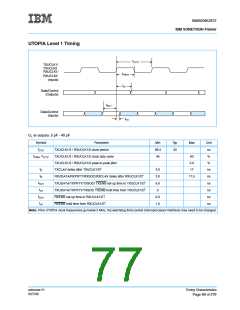
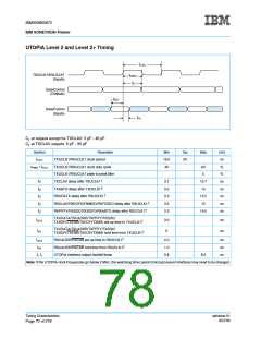
C at outputs: 3 pF - 25 pF
L
Symbol
Parameter
Min
Typ
51.44
Max
Unit
ns
tCYC
RXTB#CLK clock period
RXTB#CLK duty cycle
tPWH / tCYC
42.5
-3.5
1.3
57.5
1.0
%
RXTB#DATA(7:0)/RXTB#C1J1/
RXTB#SPE/RXTB#PAR/RXTB#FAIL delay after RXTB#CLK↑
(CKINV#=1) or after RXTB#CLK↓ (CKINV#=0)
tD
ns
tr, tf
Receive Telecom Bus interface output rise and fall times
7.5
ns
Note: The dashed line in the RXTB#C1J1 signal shows the position of the C1 pulse when the corresponding CPOS bit is set to ’0’.
When CPOS is set to ’0’, the J1 pulse is not present in the corresponding RXTB#C1J1 signal. The solid pulse in the RXTB#C1J1 signal
shows the position of the C1 pulse when the corresponding CPOS bit is set to a ‘1’. When CPOS is set to ‘1’, the J1 pulse is present in
the corresponding RXTB#C1J1 signal. The J1 pulse is not shown in the timing diagram but has the same timing parameters as the C1
pulse.
ssframer.01
8/27/99
Timing Characteristics
Page 73 of 279

 IBM [ IBM ]