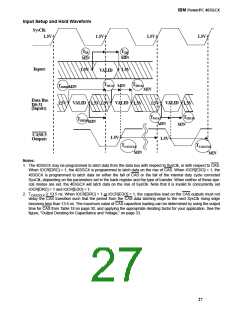
IBM PowerPC 403GCX
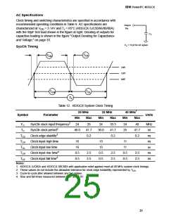
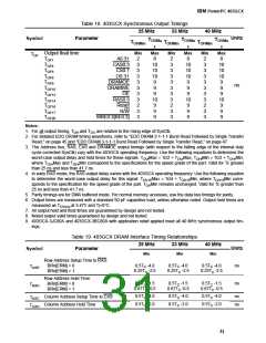
All TIS and TIH timings in Table 16 are specified with respect to the rise of the external SysClk signal.
Internal system clocks are duty-cycle corrected so the falling edge of the external SysClk signal may not
be the same as the falling edge of the internally corrected system clock.
Table 16. 403GCX Synchronous Input Timings
25 MHz
33 MHz
40 MHz6
Symbol
Parameter
Units
Min Max
Min Max
Min Max
TIS
Input setup:
TIS1
A4:11,A22:31
BusError
3
5
4
23
3
3
3
5
4
18
3
3
3
5
4
15.5
3
3
TIS2
TIS3
TISEDO
TISCAS
TIS4
D0:31 (to SysClk)3
D0:31 (to SysClk)4,5
D0:31 (to CAS)5
HoldPri
ns
TIS5
HoldReq
3
3
3
TIS6
R/W
3
3
3
TIS7
Ready
6
5
5
TIS8
TIS9
Ready(SOR mode)
XReq
12
5
11
4
10
4
TIS10
XSize0:1
4
3
3
TIH
Input hold:
TIH1
A4:11,A22:31
BusError
2
2
3
2
2
3
-12
3
2
2
2
2
2
2
2
3
-9.5
3
2
2
2
2
2
TIH2
TIH3
TIHEDO
TIHCAS
TIH4
TIH5
TIH6
TIH7
TIH8
D0:31 (after SysClk)3
D0:31 (after SysClk)4,5 -17
D0:31 (after CAS)5
HoldPri
3
2
2
2
2
2
2
2
ns
ns
HoldReq
R/W
Ready
Ready(SOR mode)
XReq
TIH9
TIH10
2
2
2
2
XSize0:1
TR,TF Input rise/fall time
0.5
2.5
0.5
2.5
0.5
2.5
Notes:
1. Parity setup and hold times are the same as for the data bus.
2. For detailed EDO DRAM timing waveforms, refer to "EDO DRAM 2-1-1-1 Burst Read Followed by Single Transfer
Read," on page 45 and "EDO DRAM 3-1-1-1 Burst Read Followed by Single Transfer Read," on page 47.
3. Data bus input setup and hold times TIS3 and TIH3 are the specifications to use for all modes except DRAM Read
on CAS and EDO DRAM read modes (controlled via IOCR[DRC] and IOCR[EDO], respectively).
4. In EDO mode, the data bus input setup and hold times with respect to SysClk. Use the following equations to
determine the minimum input setup and hold times for this signal: TISEDOMin = Tc/2 + 3; TIHEDOMin = -Tc/2 + 3.
Valid for Tc greater than 25ns and less than 41.7 ns.
5. Guaranteed by design and not tested.
6. 403GCX-3JC80A and 403GCX-3BC80A with application relief applied meet all 40 MHz synchronous input timings.
28

 IBM [ IBM ]