IBM PowerPC 403GCX
40 MHz
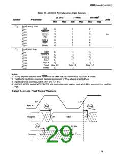
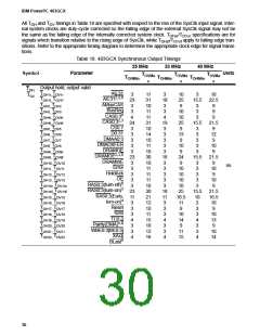
Table 18. 403GCX Synchronous Output Timings
25 MHz 33 MHz
Units
Symbol
Parameter
TOVMa
TOVMa
TOVMa
TOHMin
TOHMin
TOHMin
x
x
x
Output float time
TOF1
TOF4
TOF5
TOF6
TOF9
TOF10
TOF13
TOF14
TOF16
TOF17
TOF20
Min
2
3
3
3
3
3
3
3
Max
8
10
10
10
9
9
9
10
9
9
Min
2
3
3
3
3
3
3
3
Max
8
10
10
10
9
9
9
10
9
9
Min
2
3
3
3
3
3
3
3
Max
8
10
10
10
9
9
9
10
9
9
TOF
A6:31
CAS0:3
CS0:7
D0:31
DRAMOE
DRAMWE
OE
RAS0:3
Reset
ns
2
3
3
2
3
3
2
3
3
R/W
WBE0:3[BE0:3]
9
9
9
Notes:
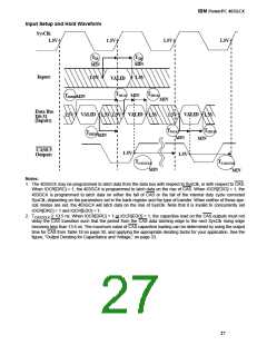
1. For all output timing, T and T are relative to the rising edge of SysClk.
OH
OV
2. For detailed EDO DRAM timing waveforms, refer to "EDO DRAM 2-1-1-1 Burst Read Followed by Single Transfer
Read," on page 45 and "EDO DRAM 3-1-1-1 Burst Read Followed by Single Transfer Read," on page 47.
3. The Address bus, RAS, CAS and DRAMOE output timings (with respect to the falling edge of the internal duty
cycle corrected SysClk) vary with the 403GCX operating frequency. Use the following equations to determine the
worst-case output delay and hold times for these signals: T Max = Tc/2 + T Max; T Min = Tc/2 + T Min,
OVf
OVr
OHf
OHr
where T Max and T Min correspond to the specifications for the speed grade of the part. Valid for Tc greater
OVr
OHr
than 25 ns and less than 41.7 ns.
4. In early RAS mode, the RAS output delay varies with the 403GCX operating frequency. Use the following equation
to determine the worst-case output delay for this signal: T
Max = Tc/4 + T
Min, where T
Min corre-
OV15
OH15
OH15
sponds to the specification for the speed grade of the part. T Min remains unchanged. Valid for Tc greater than
OH
25 ns and less than 41.7 ns.
5. Parity timings are for DMA buffered mode. For normal memory accesses, use the data bus timings for parity.
6. Output times are measured with a standard 50 pF capacitive load, unless otherwise noted. Output hold times are
measured as T
at 3.47V and Tj=0°C.
OVmin
7. All output hold and float times are guaranteed by design and not tested.
8. Noted output valid times guaranteed by design and not tested.
9. 403GCX-3JC80A and 403GCX-3BC80A with application relief applied meet all 40 MHz synchronous output tim-
ings.
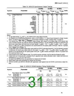
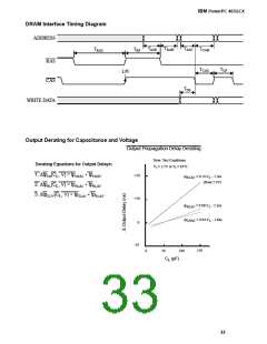
Table 19. 403GCX DRAM Interface Timing Relationships
25 MHz
33 MHz
40 MHz
Units
Symbol
Parameter
Min
Min
Min
Row Address Setup Time to RAS:
BRn[ERM] = 0
BRn[ERM] = 1
0.5T -4.0
0.5T -4.0
0.5T -4.0
ns
T
C
C
C
ASR
0.25T -2.5
0.25T -2.5
0.25T -2.5
C
C
C
Row Address Hold Time:
BRn[ERM] = 0
BRn[ERM] = 1
0.5T -1.5
0.5T -1.5
0.5T -1.5
ns
T
C
C
C
RAH
0.67T -0.5
0.67T -0.5
0.67T -0.5
C
C
C
0.5T -4.0
0.5T -4.0
0.5T -4.0
ns
ns
Column Address Setup Time to CAS
Column Address Hold Time
T
C
C
C
ASC
0.5T -2.0
0.5T -2.0
0.5T -2.0
T
C
C
C
CAH
31

 IBM [ IBM ]