IBM PowerPC 403GCX
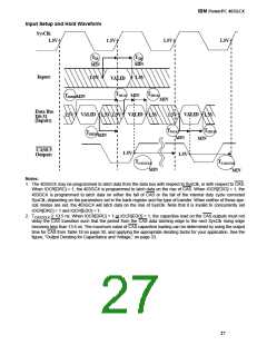
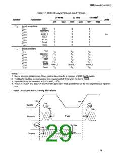
Input Setup and Hold Waveform
SysClk
1.5V+
1.5V+
1.5V+
1.5V+
TIS
TIH
MIN
MIN
Inputs
+ 1.5V
1.5V +
VALID
TISCAS
TIHCAS
MIN
TISEDOMIN
MIN
Data Bus
VALID
(Inputs)
VALID
VALID
1.5V+
+1.5V 1.5V+
+1.5V
1.5V+
TISCAS
+1.5V
TIHCAS
D0:31
TIHEDO
MIN
MIN
MIN
CAS0:3
Outputs
1.5V+
TCAS2CLK
1.5V+
TCAS2CLK
MIN
MIN
Notes:
1. The 403GCX may be programmed to latch data from the data bus with respect to SysClk, or with respect to CAS.
When IOCR[DRC] = 1, the 403GCX is programmed to latch data on the rise of CAS. When IOCR[EDO] = 1, the
403GCX is programmed to latch data on either the fall of CAS or the fall of the internal duty cycle corrected
SysClk, depending on the parameters set in the bank register and the type of transfer. When neither of these spe-
cial modes are set, the 403GCX will latch data on the rise of SysClk. Note that it is invalid to concurrently set
IOCR[DRC] = 1 and IOCR[EDO] = 1.
2. TCAS2CLK ≥ 13.5 ns. When IOCR[DRC] = 1 or IOCR[EDO] = 1, the capacitive load on the CAS outputs must not
delay the CAS transition such that the period from the CAS data latching edge to the next SysClk rising edge
becomes less than 13.5 ns. The maximum value of CAS capacitive loading can be determined by using the output
time for CAS from Table 18 on page 30, and applying the appropriate derating factor for your application. See the
figure, "Output Derating for Capacitance and Voltage," on page 33.
27

 IBM [ IBM ]