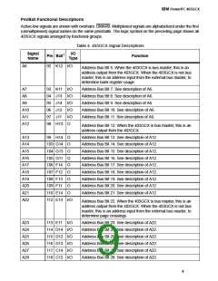
IBM PowerPC 403GCX
and for DRAM, SRAM, or ROM banks are pro-
vided by the BIU. Burst access for SRAM, ROM,
and page-mode DRAM devices is supported for
cache fill and flush operations.
ble. For each SRAM/ROM bank, the bank size,
bank location, number of wait states, and timings
of chip selects, byte enables, and output enables
are all user-programmable.
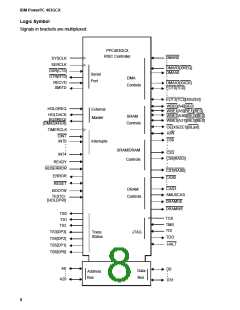
The BIU controls the transfer of data between the
external bus and the instruction cache, the data
cache, or registers internal to the processor core.
The BIU also arbitrates among external bus mas-
ter and DMA transfers, the internal buses to the
cache units and the register banks, and the serial
port on the on-chip peripheral bus (OPB).
Memory Management Unit
The memory management unit (MMU) supports
address translation and protection functions for
embedded applications. When used with appro-
priate system level software, the MMU provides
the following functions: translation of 4GB logical
address space into physical addresses, indepen-
dent enabling of instruction and data translation/
protection, page level cacheability and access
control via the translation mechanism, software
control of page replacement strategy, and addi-
tional control over protection via zones.
Memory Addressing Regions
The 403GCX can address an effective range of
four gigabytes, mapped to 3.5GB (256MB for
SRAM/ROM or other I/O, 256MB DRAM, and
3GB OPB/reserved) of physical address space
containing twenty-eight 128MB regions. Cache-
ability with respect to the instruction or data
cache is programmed via the instruction and data
cache control registers, respectively.
The fully associative 64-entry TLB array handles
both instruction and data accesses. The transla-
tion for any virtual address can be placed in any
one of the 64 entries, allowing maximum flexibil-
ity by TLB management software. Each TLB
entry contains a translation for a page that can
be any one of eight sizes from 1KB to 16MB,
incrementing by powers of 4.
Within the DRAM and SRAM/ROM regions, a
total of eight banks of devices are supported.
Each bank can be configured for 8-, 16-, or 32-bit
devices.
The TLB can simultaneously contain any mix of
page sizes. This feature enables the use of small
pages when maximum granularity is required,
reducing the amount of wasted memory when
compared to the more common fixed 4KB page
For individual DRAM banks, the number of wait
states, bank size, RAS-to-CAS timing, use of an
external address multiplexer (for external bus
masters), and refresh rate are user-programma-
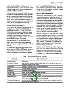
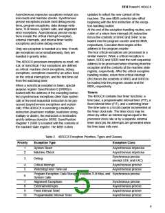
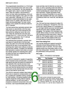
Table 1. 403GCX Instructions by Category
Base Instructions
Category
Data Movement
load, store
Arithmetic / Logical
add, subtract, negate, multiply, divide, and, or, xor, nand, nor, xnor, sign
extension, count leading zeros
Comparison
Branch
compare, compare logical, compare immediate
branch, branch conditional
Condition
condition register logical
Rotate/Shift
Cache Control
Interrupt Control
rotate, rotate and mask, shift left, shift right
invalidate, touch, zero, flush, store
write to external interrupt enable bit, move to/from machine state register,
return from interrupt, return from critical interrupt
Processor Management system call, synchronize, move to/from device control registers, move to/
from special purpose registers
3

 IBM [ IBM ]