IBM PowerPC 403GCX
Pin/Ball Functional Descriptions
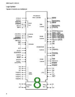
Active-low signals are shown with overbars: DMAR0. Multiplexed signals are alphabetized under the first
(unmultiplexed) signal names on the same pins/balls. The logic symbol on the preceding page shows all
403GCX signals arranged by functional groups.
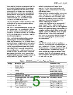
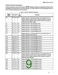
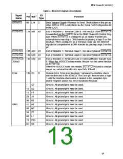
Table 4. 403GCX Signal Descriptions
Signal
Name
I/O
Type
Pin Ball1
Function
A6
92 K12 I/O
Address Bus Bit 6. When the 403GCX is bus master, this is an
address output from the 403GCX. When the 403GCX is not bus
master, this is an address input from the external bus master, to
determine bank register usage.
A7
A8
A9
93 K11 I/O
94 J13 I/O
95 J14 I/O
96 J12 I/O
97 J11 I/O
Address Bus Bit 7. See description of A6.
Address Bus Bit 8. See description of A6.
Address Bus Bit 9. See description of A6.
Address Bus Bit 10. See description of A6.
Address Bus Bit 11. See description of A6.
A10
A11
A12
98 H13
O
Address Bus Bit 12. When the 403GCX is bus master, this is an
address output from the 403GCX.
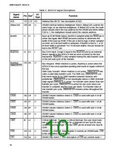
A13
A14
A15
A16
A17
A18
A19
A20
A21
A22
99 H14
103 G14
104 G13
105 G11
106 F14
107 F12
108 F13
109 F11
110 E14
O
O
O
O
O
O
O
O
O
Address Bus Bit 13. See description of A12.
Address Bus Bit 14. See description of A12.
Address Bus Bit 15. See description of A12.
Address Bus Bit 16. See description of A12.
Address Bus Bit 17. See description of A12.
Address Bus Bit 18. See description of A12.
Address Bus Bit 19. See description of A12.
Address Bus Bit 20. See description of A12.
Address Bus Bit 21. See description of A12.
112 E13 I/O
Address Bus Bit 22. When the 403GCX is bus master, this is an
address output from the 403GCX. When the 403GCX is not bus
master, this is an address input from the external bus master, to
determine page crossings.
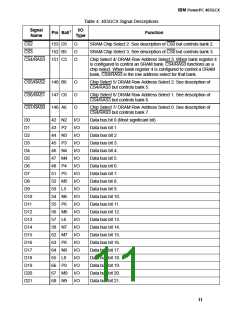
A23
A24
A25
A26
A27
A28
113 E11 I/O
114 D14 I/O
115 D12 I/O
116 D13 I/O
117 C14 I/O
118 C12 I/O
Address Bus Bit 23. See description of A22.
Address Bus Bit 24. See description of A22.
Address Bus Bit 25. See description of A22.
Address Bus Bit 26. See description of A22.
Address Bus Bit 27. See description of A22.
Address Bus Bit 28. See description of A22.
9

 IBM [ IBM ]