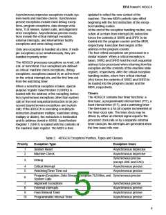
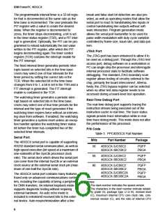
IBM PowerPC 403GCX
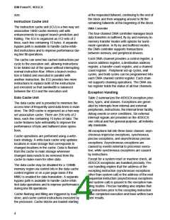
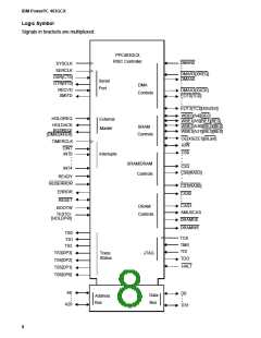
The 403GCX RISC controller consists of a pipe-
lined RISC processor core and several peripheral
interface units: BIU, DMA controller, asynchro-
nous interrupt controller, serial port, and JTAG
debug port.
the address for the data read or write to the
BIU.When noncacheable operands are being
transferred, data can pass directly between the
EXU and the BIU, which interfaces to the exter-
nal memory being accessed.
The RISC processor core includes the internal
16KB instruction cache and 8KB data cache,
reducing overhead for data transfers to or from
external memory. The instruction queue logic
manages branch prediction, folding of branch
and condition register logical instructions, and
instruction prefetching to minimize pipeline
stalls.The integrated memory management unit
provides robust memory management and pro-
tection functions, optimized for embedded envi-
ronments.
Special Purpose Registers
Special purpose registers are used to control
debug facilities, timers, interrupts, the protection
mechanism, memory cacheability, and other
architected processor resources. SPRs are
accessed using move to/from special purpose
register (mtspr/mfspr) instructions, which move
operands between GPRs and SPRs.
Supervisory programs can write the appropriate
SPRs to configure the operating and interface
modes of the execution unit. The condition regis-
ter (CR) and machine state register (MSR) are
written by internal control logic with program exe-
cution status and machine state, respectively.
Status of external interrupts is maintained in the
external interrupt status register (EXISR). Fixed-
point arithmetic exception status is available from
the exception register (XER).
RISC CPU
The RISC core comprises four tightly coupled
functional units: the execution unit (EXU), the
memory management unit (MMU), the data
cache unit (DCU), and the instruction cache unit
(ICU). Each cache unit consists of a data array,
tag array, and control logic for cache manage-
ment and addressing. The execution unit con-
sists of general purpose registers (GPR), special
purpose registers (SPR), ALU, multiplier, divider,
barrel shifter, and the control logic required to
manage data flow and instruction execution
within the EXU. The 403GCX core can operate at
either 1X or 2X the speed of the external buses,
which run at the SysClk input rate.
Device Control Registers
Device control registers (DCR) are used to man-
age I/O interfaces, DMA channels, SRAM and
DRAM memory configurations and timing, and
status/address information regarding bus errors.
DCRs are accessed using move to/from device
control register (mtdcr/mfdcr) instructions, which
move operands between GPRs and DCRs.
The EXU handles instruction decoding and exe-
cution, queue management, branch prediction,
and branch folding. The instruction cache unit
passes instructions to the queue in the EXU or, in
the event of a cache miss, requests a fetch from
external memory through the bus interface unit.
The MMU provides translation and memory pro-
tection for instruction and data accesses, using a
unified 64-entry, fully associative TLB array.
Instruction Set
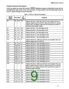
Table 1 summarizes the 403GCX instruction set
by categories of operations. Most instructions
execute in a single cycle, with the exceptions of
load/store multiple, load/store string, multiply,
and divide instructions.
Bus Interface Unit
General Purpose Registers
The bus interface unit integrates the functional
controls for data transfers and address opera-
tions other than those which the DMA controller
handles. DMA transfers use the address logic in
the BIU to output the memory addresses being
accessed.
Data transfers to and from the EXU are handled
through the bank of 32 GPRs, each 32 bits wide.
Load and store instructions move data operands
between the GPRs and the data cache unit,
except in the cases of noncacheable data or
cache misses. In such cases the DCU passes
Control functions for direct-connect I/O devices
2

 IBM [ IBM ]