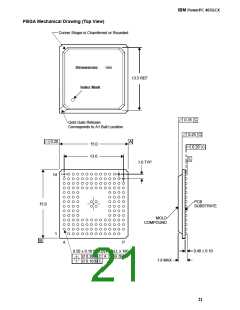
IBM PowerPC 403GCX
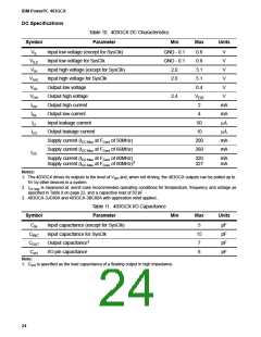
AC Specifications
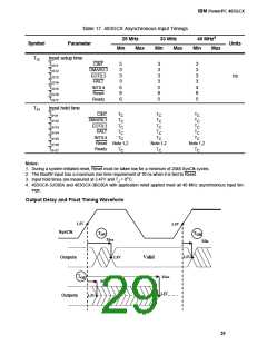
Clock timing and switching characteristics are specified in accordance with
recommended operating conditions in Table 9. AC specifications are
characterized at VDD = 3.14V and TJ = 85°C (403GCX-3JC50/66/80/80A)
with the 50pF test load shown in the figure at right. Derating of outputs for
capacitive loading is shown in the figure "Output Derating for Capacitance
and Voltage," on page 33.
Output
Pin
CL
CL = 50 pf for all signals
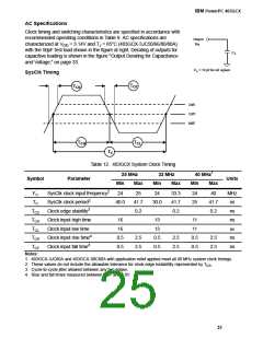
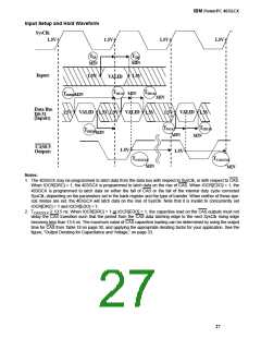
SysClk Timing
T
T
CF
CR
2.0V
1.5V
0.8V
T
T
CL
CH
T
C
Table 12. 403GCX System Clock Timing
25 MHz 33 MHz
40 MHz1
Symbol
Parameter
Units
Min
Max
Min
Max
Min
Max
FC
TC
SysClk clock input frequency2
SysClk clock period2
Clock edge stability3
Clock input high time
Clock input low time
Clock input rise time4
Clock input fall time4
24
25
41.7
0.2
24
33.3
41.7
0.2
24
25
40
41.7
0.2
MHz
ns
40.0
30.0
TCS
TCH
TCL
TCR
ns
16
16
13
13
11
11
ns
ns
0.5
0.5
2.5
2.5
0.5
0.5
2.5
2.5
0.5
0.5
2.5
2.5
ns
TCF
ns
Notes:
1. 403GCX-3JC80A and 403GCX-3BC80A with application relief applied meet all 40 MHz system clock timings.
2. These values do not include the allowable tolerance for clock edge instablility represented by T
3. Cycle-to-cycle jitter allowed between any two edges.
.
CS
4. Rise and fall times measured between 0.8V and 2.0V.
25

 IBM [ IBM ]