IBM PowerPC 403GCX
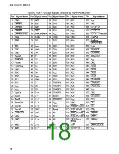
Signal
Table 4. 403GCX Signal Descriptions
I/O
Type
Pin Ball1
Function
Name
90 K13
101 G12
102 H12
111 E12
121 G8
130 B10
141 C7
150 A5
Ground. All ground pins must be used.
Ground. All ground pins must be used.
Ground. All ground pins must be used.
Ground. All ground pins must be used.
Ground. All ground pins must be used.
Ground. All ground pins must be used.
Ground. All ground pins must be used.
Ground. All ground pins must be used.
Halt from external debugger, active low.
GND
Halt
9
D4
I
HoldAck
134 B9
14 F2
31 K3
O
Hold Acknowledge. HoldAck outputs a logic 1 when the 403GCX
relinquishes its external buses to an external bus master. HoldAck
outputs a logic 0 when the 403GCX regains control of the bus.
HoldReq
INT0
I
Hold Request. External bus masters can request the 403GCX bus
by placing a logic1 on this pin. The external bus master relinquishes
the bus to the 403GCX by deasserting HoldReq.
I
Interrupt 0. INT0 is an interrupt input to the 403GCX and users
may program the pin to be either edge-triggered or level-triggered
and may also program the polarity to be active high or active low.
The IOCR contains the bits necessary to program the trigger type
and polarity.
INT1
INT2
INT3
INT4
IVR
32 K2
33 K4
34 L1
35 L3
39 M2
I
I
I
I
I
Interrupt 1. See description of INT0.
Interrupt 2. See description of INT0.
Interrupt 3. See description of INT0.
Interrupt 4. See description of INT0.
Reserved for manufacturing test. Tied high for normal operation.
OE/XSize1/ 126 B11 O/I/O Output Enable / External Master Transfer Size 1. When the 403GCX
BLast
is bus master, OE enables the selected SRAMs to drive the data
bus. The timing parameters of OE relative to the chip select, CS, are
programmable via bits in the 403GCX bank registers.
When the 403GCX is not bus master, OE/XSize1 is used as one of
two external transfer size input bits, XSize0:1.
In Byte Enable mode, Burst Last (BLast) goes active to indicate the
last transfer of a memory access, whether burst or nonburst.
Ready
RecvD
13 E4
27 J3
I
I
Ready. Ready is used to insert externally generated (device-paced)
wait states into bus transactions. The Ready pin is enabled via the
Ready Enable bit in 403GCX bank registers.
Serial Port Receive Data.
14

 IBM [ IBM ]