IBM PowerPC 403GCX
Signal
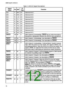
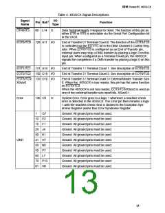
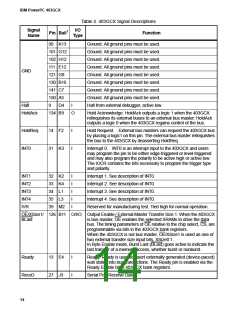
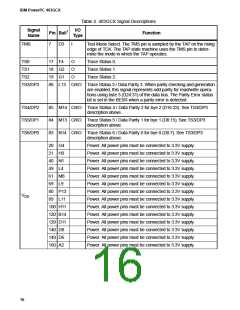
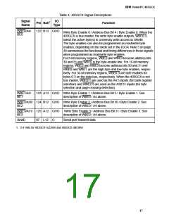
Table 4. 403GCX Signal Descriptions
I/O
Type
Pin Ball1
D3
Function
Name
TMS
7
I
Test Mode Select. The TMS pin is sampled by the TAP on the rising
edge of TCK. The TAP state machine uses the TMS pin to deter-
mine the mode in which the TAP operates.
TS0
17 F4
18 G2
19 G1
O
O
O
Trace Status 0.
Trace Status 1.
Trace Status 2.
TS1
TS2
TS3/DP3
86 L13 O/I/O Trace Status 3 / Data Parity 3. When parity checking and generation
are enabled, this signal represents odd parity for read/write opera-
tions using byte 3 (D24:31) of the data bus. The Parity Error status
bit is set in the BESR when a parity error is detected.
TS4/DP2
TS5/DP1
TS6/DP0
85 M14 O/I/O Trace Status 4 / Data Parity 2 for bye 2 (D16:23). See TS3/DP3
description above.
84 M13 O/I/O Trace Status 5 / Data Parity 1 for bye 1 (D8:15). See TS3/DP3
description above.
83 N14 O/I/O Trace Status 6 / Data Parity 0 for bye 0 (D0:7). See TS3/DP3
description above.
20 G4
21 H3
40 N1
49 L4
61 M8
69 L9
80 P13
89 L11
100 H11
120 B14
129 D11
140 D8
149 D6
160 A2
Power. All power pins must be connected to 3.3V supply.
Power. All power pins must be connected to 3.3V supply.
Power. All power pins must be connected to 3.3V supply.
Power. All power pins must be connected to 3.3V supply.
Power. All power pins must be connected to 3.3V supply.
Power. All power pins must be connected to 3.3V supply.
Power. All power pins must be connected to 3.3V supply.
Power. All power pins must be connected to 3.3V supply.
Power. All power pins must be connected to 3.3V supply.
Power. All power pins must be connected to 3.3V supply.
Power. All power pins must be connected to 3.3V supply.
Power. All power pins must be connected to 3.3V supply.
Power. All power pins must be connected to 3.3V supply.
Power. All power pins must be connected to 3.3V supply.
VDD
16

 IBM [ IBM ]