IBM PowerPC 403GCX
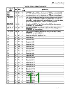
Signal
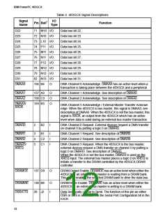
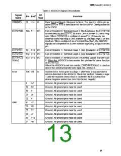
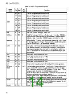
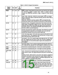
Table 4. 403GCX Signal Descriptions
I/O
Type
Pin Ball1
Function
Name
D22
71 M10 I/O
Data bus bit 22.
Data bus bit 23.
Data bus bit 24.
Data bus bit 25.
Data bus bit 26.
Data bus bit 27.
Data bus bit 28.
Data bus bit 29.
Data bus bit 30.
Data bus bit 31.
D23
D24
D25
D26
D27
D28
D29
D30
D31
DMAA0
72 N10 I/O
73 L10 I/O
74 P11 I/O
75 M11 I/O
76 N11 I/O
77 P12 I/O
78 M12 I/O
79 N12 I/O
82 N13 I/O
156 B4
O
DMA Channel 0 Acknowledge. DMAA0 has an active level when a
transaction is taking place between the 403GCX and a peripheral.
DMAA1
DMAA2
157 A3
158 C3
159 B3
O
O
O
DMA Channel 1 Acknowledge. See description of DMAA0.
DMA Channel 2 Acknowledge. See description of DMAA0.
DMAA3/
XACK
DMA Channel 3 Acknowledge / External Master Transfer Acknowl-
edge. When the 403GCX is bus master, this signal is DMAA3; see
description of DMAA0. When the 403GCX is not the bus master, this
signal is XACK, an output from the 403GCX which has an active
level when data is valid during an external bus master transaction.
DMAR0
2
B2
I
DMA Channel 0 Request. External devices request a DMA transfer
on channel 0 by putting a logic 0 on DMAR0.
DMAR1
DMAR2
3
4
5
B1
C2
C1
I
I
I
DMA Channel 1 Request. See description of DMAR0.
DMA Channel 2 Request. See description of DMAR0.
DMAR3/
XREQ
DMA Channel 3 Request. When the 403GCX is the bus master,
external devices request a DMA transfer on channel 3 by putting a
logic 0 on DMAR3. See description of DMAR0.
When the 403GCX is not the bus master, DMAR3 is used as the
XREQ input. The external bus master places a logic 0 on XREQ to
initiate a transfer to the DRAM controlled by the 403GCX DRAM
controller.
DRAMOE
137 D9
O
DRAM Output Enable. DRAMOE has an active level when either the
403GCX or an external bus master is reading from a DRAM bank.
This signal enables the selected DRAM bank to drive the data bus.
DRAMWE
DSR/CTS
138 B8
28 J2
O
I
DRAM Write Enable. DRAMWE has an active level when either the
403GCX or an external bus master is writing to a DRAM bank.
Data Set Ready / Clear to Send. The function of this pin as either
DSR or CTS is selectable via the Serial Port Configuration bit in the
IOCR.
12

 IBM [ IBM ]