IBM PowerPC 403GCX
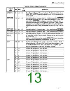
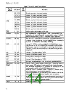
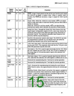
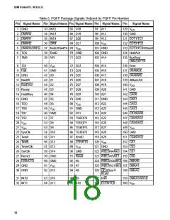
Table 4. 403GCX Signal Descriptions
Signal
Name
I/O
Type
Pin Ball1
Function
WBE0/A4/
BE0
122 B13 O/I/O
Write Byte Enable 0 / Address Bus Bit 4 / Byte Enable 0. When the
403GCX is bus master, the write byte enable outputs, WBE0:3,
select the active byte(s) in a memory write access to SRAM.
The byte enables can also be programmed as read/write byte
enables, depending on the mode set in the IOCR. Note 3 on page
38 summarizes the functional and timing differences in these signals
when programmed as read/write byte enables.
For 8-bit memory regions, WBE2 and WBE3 become address bits
30 and 31 and WBE0 is the byte-enable line. For 16-bit memory
regions, WBE2 and WBE3 become address bits 30 and 31 and
WBE0 and WBE1 are the high byte and low byte enables, respec-
tively. For 32-bit memory regions, WBE0:3 are byte enables for
bytes 0-3 on the data bus, respectively. When the 403GCX is not
bus master, WBE0:1 are used as the A4:5 inputs (for bank register
selection) and WBE2:3 are used as the A30:31 inputs (for byte
selection and page crossing detection).
WBE1/A5/
BE1
123 A13 O/I/O Write Byte Enable 1 / Address Bus Bit 5 / Byte Enable 1. See
description of WBE0 / A4 above.
WBE2/A30/ 124 B12 O/I/O Write Byte Enable 2 / Address Bus Bit 30 / Byte Enable 2. See
BE2
description of WBE0 / A4 above.
WBE3/A31/ 125 A12 O/I/O
BE3
Write Byte Enable 3 / Address Bus Bit 31 / Byte Enable 3. See
description of WBE0 / A4 above.
XmitD
87 L12
O
Serial port transmit data.
1. 3.4 Volts for 403GCX-3JC80A and 403GCX-3BC80A
17

 IBM [ IBM ]