IBM PowerPC 403GCX
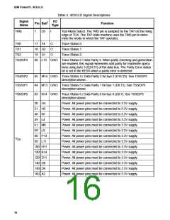
Table 4. 403GCX Signal Descriptions
Signal
Name
I/O
Type
Pin Ball1
Function
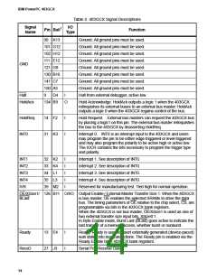
Reset
91 K14 I/O
Reset. A logic 0 input placed on this pin for one SysClk cycle causes
the 403GCX to begin a system reset. When a system reset is
invoked, the Reset pin becomes a logic 0 output for 2048 SysClk
cycles.
R/W
127 C11 I/O
Read / Write. When the 403GCX is bus master, R/W is an output
which is high when data is read from memory and low when data is
written to memory.
When the 403GCX is not bus master, R/W is an input from the
external bus master which indicates the direction of data transfer.
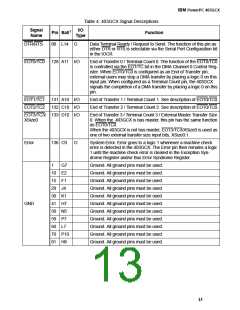
SerClk
26 J1
I
Serial Port Clock. Through the Serial Port Clock Source bit in the
Input/Output Configuration register (IOCR), users may choose the
serial port clock source from either the input on the SerClk pin or
processor SysClk. The maximum allowable input frequency into
SerClk is half the SysClk frequency.
SysClk
TCK
22 G3
I
I
I
SysClk is the processor system clock input. The 403GCX can also
be programmed to operate at a 2X internal clock rate while the
external bus interface runs at the SysClk input rate.
6
8
D2
D1
JTAG Test Clock Input. TCK is the clock source for the 403GCX test
access port (TAP). The maximum clock rate into the TCK pin is one
half of the processor SysClk clock rate.
TDI
Test Data In. The TDI is used to input serial data into the TAP. When
the TAP enables the use of the TDI pin, the TDI pin is sampled on
the rising edge of TCK and this data is input to the selected TAP
shift register.
TDO
16 F3
O
Test Data Output. TDO is used to transmit data from the 403GCX
TAP. Data from the selected TAP shift register is shifted out on TDO.
TestA
TestB
23 H1
24 H2
I
I
I
Reserved for manufacturing test. Tied low for normal operation.
Reserved for manufacturing test. Tied high for normal operation.
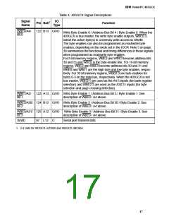
TestC/Hold- 37 M1
Pri
TestC. Reserved for manufacturing test during the reset interval.
While Reset is active, this signal should be tied low for normal oper-
ation.
HoldReq Priority. When Reset is not active, this signal is sampled to
determine the priority of the external bus master signal HoldReq. If
HoldPri = 0 then the HoldReq signal is considered high priority, oth-
erwise HoldReq is considered low priority.
TestD
38 M3
25 H4
I
I
Reserved for manufacturing test. Tied low for normal operation.
TimerClk
Timer Facility Clock. Through the Timer Clock Source bit in the
Input/Output Configuration register (IOCR), users may choose the
clock source for the Timer facility from either the input on the Timer-
Clk pin or processor CoreClk. The maximum input frequency into
TimerClk is half the CoreClk frequency.
15

 IBM [ IBM ]