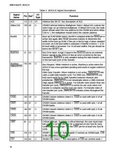
IBM PowerPC 403GCX
Signal
Table 4. 403GCX Signal Descriptions
I/O
Type
Pin Ball1
Function
Name
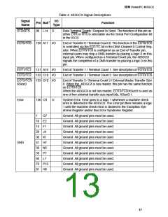
A29
119 C13 I/O
Address Bus Bit 29. See description of A22.
AMuxCAS
BootW
139 A8
11 E1
O
DRAM External Address Multiplexer Select. AMuxCAS controls the
select logic on an external multiplexer. If AMuxCAS is low, the multi-
plexer should select the row address for the DRAM and when AMux-
CAS is 1, the multiplexer should select the column address.
I
Boot-up ROM Width Select. BootW is sampled while the Reset pin is
active and again after Reset becomes inactive to determine the
width of the boot-up ROM. If this pin is tied to logic 0 when sampled
on reset, an 8-bit boot width is assumed. If BootW is tied to 1, a 32-
bit boot width is assumed. For 16-bit boot widths, this pin should be
tied to the RESET pin.
BusError
12 E3
135 A9
I
Bus Error Input. A logic 0 input to the BusError pin by an external
device signals to the 403GCX that an error occurred on the bus
transaction. BusError is only sampled during the data transfer cycle
or the last wait cycle of the transfer.
BusReq/
DMADXFER
O
Bus Request. While HoldAck is active, BusReq is active when the
403GCX has a bus operation pending and needs to regain control of
the bus.
DMA Data Transfer. When HoldAck is not active, DMADXFER indi-
cates a valid data transfer cycle. For DMA use, DMADXFER con-
trols burst-mode fly-by DMA transfers between memory and
peripherals. DMADXFER is not meaningful unless a DMA Acknowl-
edge signal (DMAA0:3) is active. For transfer rates slower than one
transfer per cycle, DMADXFER is active for one cycle when one
transfer is complete and the next one starts. For transfer rates of
one transfer per cycle, DMADXFER remains active throughout the
transfer.
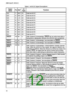
CAS0
CAS1
CAS2
CAS3
CINT
142 C8
143 A7
144 B7
145 D7
36 L2
O
O
O
O
I
DRAM Column Address Select 0. CAS0 is used with byte 0 of all
DRAM banks.
DRAM Column Address Select 1. CAS1 is used with byte 1 of all
DRAM banks.
DRAM Column Address Select 2. CAS2 is used with byte 2 of all
DRAM banks.
DRAM Column Address Select 3. CAS3 is used with byte 3 of all
DRAM banks.
Critical Interrupt. To initiate a critical interrupt, the user must main-
tain a logic 0 on the CINT pin for a minimum of one SysClk clock
cycle followed by a logic 1 on the CINT pin for at least one SysClk
cycle.
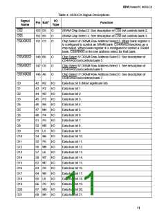
CS0
CS1
155 C4
154 A4
O
O
SRAM Chip Select 0. Bank register 0 controls an SRAM bank, CS0
is the chip select for that bank.
SRAM Chip Select 1. See description of CS0 but controls bank 1.
10

 IBM [ IBM ]