APCPCWM_4828539:WP_0000001WP_0000001
1
H27(U_S)4G8_6F2D
4 Gbit (512M x 8 bit) NAND Flash
2. BUS OPERATION
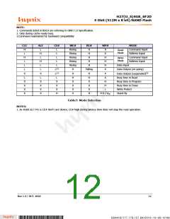
There are six standard bus operationTable 28s that control the device. These are Command Input, Address Input, Data
Input, Data Output, Write PrTable 28otect, and Standby. (see Figure 1 and Table 6)
Typically glitches less than 5 ns on Chip Enable, Write Enable and Read Enable are ignored by the memory and do not
affect bus operations.
2.1. Command Input
Command Input bus operation is used to give a command to the memory device. Command are accepted with Chip
Enable low, Command Latch Enable High, Address Latch Enable low and Read Enable High and latched on the rising
edge of Write Enable. Moreover for commands that starts a modify operation (write/erase) the Write Protect pin must
be high. See Figure 5 and Table 28 for details of the timings requirements. Command codes are always applied on
IO7:0 regardless of the bus configuration. (X8 or X16)
2.2. Address Input
Address Input bus operation allows the insertion of the memory address. 5 clock cycles are needed to input the
addresses. Addresses are accepted with Chip Enable low, Address Latch Enable High, Command Latch Enable low and
Read Enable High and latched on the rising edge of Write Enable. Moreover for commands that starts a modify opera-
tion (write/erase) the Write Protect pin must be high. See Figure 5 and Table 28 for details of the timings require-
ments. Addresses are always applied on IO7:0 regardless of the bus configuration. (X8 or X16). Refer to Table 4 and
Table 5 for more detailed information.
2.3. Data Input
Data Input bus operation allows to feed to the device the data to be programmed. The data insertion is serial and
timed by the Write Enable cycles. Data are accepted only with Chip Enable low, Address Latch Enable low, Command
Latch Enable low, Read Enable High, and Write Protect High and latched on the rising edge of Write Enable. See Fig-
ure 7 and Table 28 for details of the timings requirements.
2.4. Data Output
Data Output bus operation allows to read data from the memory array and to check the status register content, the
EDC register content and the ID data. Data can be serially shifted out by toggling the Read Enable pin with Chip Enable
low, Write Enable High, Address Latch Enable low, and Command Latch Enable low. See Figure 8 to Figure 11 and
Table 28 for details of the timings requirements.
2.5. Write Protect
Hardware Write Protection is activated when the Write Protect pin is low. In this condition modify operation do not start
and the content of the memory is not altered. Write Protect pin is not latched by Write Enable to ensure the protection
even during the power up.
2.6. Standby
In Standby the device is deselected, outputs are disabled and Power Consumption is reduced.
Rev 1.4 / OCT. 2010
13
B34416/177.179.157.84/2010-10-08 10:08
*ba53f20d-240c*

 HYNIX [ HYNIX SEMICONDUCTOR ]