APCPCWM_4828539:WP_0000001WP_0000001
1
H27(U_S)4G8_6F2D
4 Gbit (512M x 8 bit) NAND Flash
1.4 Address role
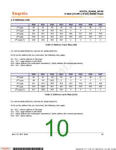
DQ0
A0
DQ1
A1
DQ2
A2
DQ3
A3
DQ4
A4
DQ5
A5
DQ6
A6
DQ7
A7
1st Cycle
A8
A9
A10
A14
A22
A30
A11
A15
A23
A31
0
0
0
0
2
nd Cycle
A12
A20
A28
A13
A21
A29
A16
A24
0
A17
A25
0
A18
A26
0
A19
A27
0
3
rd Cycle
th Cycle
4
5
th Cycle (*)
Table 4: Address Cycle Map (x8)
(*): A30 for 8Gbit DDP(1CE). A30:A31 for 16Gbit QDP(1CE).
As far as the address bits are concerned, the following rules apply:
A0 - A11 : column address in the page
A12 - A17 : page address in the block
A18 : plane address (for multi-plane operations) / block address (for normal operations)
A19 - A31 : block address
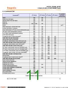
DQ0
A0
DQ1
A1
DQ2
A2
DQ3
A3
DQ4
A4
DQ5
A5
DQ6
A6
DQ7
A7
1st Cycle
nd Cycle
A8
A9
A10
A13
A21
A29
0
0
0
0
0
2
3
rd Cycle
th Cycle
A11
A19
A27
A12
A20
A28
A14
A22
A30
A15
A23
0
A16
A24
0
A17
A25
0
A18
A26
0
4
5
th Cycle (*)
Table 5: Address Cycle Map (x16)
(*): A29 for 8Gbit DDP(1CE). A29:A30 for 16Gbit QDP(1CE)
As far as the address bits are concerned, the following rules apply:
A0 - A10 : column address in the page
A11 - A16 : page address in the block
A17 : plane address (for multi-plane operations) / block address (for normal operations)
A18 - A30 : block address
Rev 1.4 / OCT. 2010
10
B34416/177.179.157.84/2010-10-08 10:08
*ba53f20d-240c*

 HYNIX [ HYNIX SEMICONDUCTOR ]