APCPCWM_4828539:WP_0000001WP_0000001
1
H27(U_S)4G8_6F2D
4 Gbit (512M x 8 bit) NAND Flash
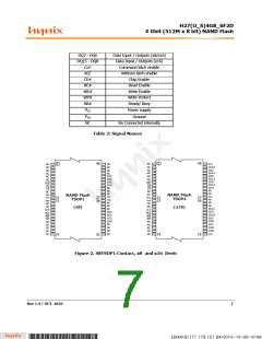
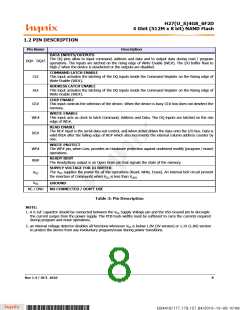
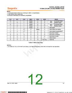
1.2 PIN DESCRIPTION
Pin Name
Description
DATA INPUTS/OUTPUTS
The DQ pins allow to input command, address and data and to output data during read / program
operations. The inputs are latched on the rising edge of Write Enable (WE#). The I/O buffer float to
High-Z when the device is deselected or the outputs are disabled.
DQ0 - DQ15
COMMAND LATCH ENABLE
CLE
ALE
This input activates the latching of the DQ inputs inside the Command Register on the Rising edge of
Write Enable (WE#).
ADDRESS LATCH ENABLE
This input activates the latching of the DQ inputs inside the Command Register on the Rising edge of
Write Enable (WE#).
CHIP ENABLE
CE#
WE#
This input controls the selection of the device. When the device is busy CE# low does not deselect the
memory.
WRITE ENABLE
This input acts as clock to latch Command, Address and Data. The DQ inputs are latched on the rise
edge of WE#.
READ ENABLE
The RE# input is the serial data-out control, and when active drives the data onto the I/O bus. Data is
valid tREA after the falling edge of RE# which also increments the internal column address counter by
one.
RE#
WRITE PROTECT
WP#
RB#
VCC
The WP# pin, when Low, provides an Hardware protection against undesired modify (program / erase)
operations.
READY BUSY
The Ready/Busy output is an Open Drain pin that signals the state of the memory.
SUPPLY VOLTAGE FOR IO BUFFER
The VCC supplies the power for all the operations (Read, Write, Erase). An internal lock circuit prevent
the insertion of Commands when VCC is less than VLKO
VSS
GROUND
NC / DNU
NO CONNECTED / DON’T USE
Table 3: Pin Description
NOTE:
1. A 0.1uF capacitor should be connected between the VCC Supply Voltage pin and the VSS Ground pin to decouple
the current surges from the power supply. The PCB track widths must be sufficient to carry the currents required
during program and erase operations.
2. an internal voltage detector disables all functions whenever VCC is below 1.8V (3V version) or 1.1V (1.8V) version
to protect the device from any involuntary program/erase during power transitions.
Rev 1.4 / OCT. 2010
8
B34416/177.179.157.84/2010-10-08 10:08
*ba53f20d-240c*

 HYNIX [ HYNIX SEMICONDUCTOR ]