APCPCWM_4828539:WP_0000001WP_0000001
1
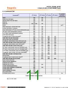
H27(U_S)4G8_6F2D
4 Gbit (512M x 8 bit) NAND Flash
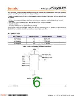
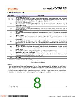
DQ7 - DQ0
DQ15 - DQ8
CLE
Data Input / Outputs (x8/x16)
Data Input / Outputs (x16)
Command latch enable
Address latch enable
Chip Enable
ALE
CE#
RE#
Read Enable
WE#
Write Enable
WP#
Write Protect
RB#
Ready/ Busy
VCC
Power supply
VSS
NC
Ground
No Connected internally
Table 2: Signal Names
1
48
NC
NC
NC
NC
NC
Vss
1
48
NC
NC
NC
NC
NC
NC
R/B
RE
NC
I/O15
I/O7
I/O14
I/O6
I/O13
I/O5
I/O12
I/O4
NC
NC
NC
NC
I/O7
I/O6
I/O5
I/O4
NC
NC
G
R/B
RE
CE
CE
NC
NC
NC
NC
Vcc
Vss
NC
NC
CLE
ALE
WE
WP
NC
NC
NC
NC
NC
NC
NC
Vcc
Vss
NC
NC
CLE
ALE
WE
WP
NC
NC
NC
NC
NC
NC
Vcc
G
NAND Flash
TSOP1
NAND Flash
TSOP1
Vcc
Vss
NC
12
13
37
36
12
13
37
36
NC
NC
NC
NC
(x16)
(x8)
I/O11
I/O3
I/O10
I/O2
I/O9
I/O1
I/O8
I/O0
Vss
NC
I/O3
I/O2
I/O1
I/O0
NC
NC
NC
NC
24
25
24
25
Figure 2. 48TSOP1 Contact, x8 and x16 Devic
Rev 1.4 / OCT. 2010
7
B34416/177.179.157.84/2010-10-08 10:08
*ba53f20d-240c*

 HYNIX [ HYNIX SEMICONDUCTOR ]