HT46R064G/065G/0662G
Enhanced A/D Type 8-Bit OTP MCU with OPA
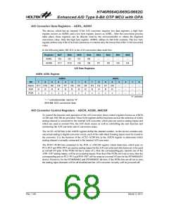
A/D Converter Data Registers - ADRL, ADRH
The device, which has an internal 12-bit A/D converter, requires two data registers, a high byte
register, known as ADRH, and a low byte register, known as ADRL. After the conversion process
takes place, these registers can be directly read by the microcontroller to obtain the digitised
conversion value. Only the high byte register, ADRH, utilises its full 8-bit contents. The low byte
register utilises only 4 bit of its 8-bit contents as it contains only the lowest bits of the 12-bit converted
value.
In the following table, D0~D11 is the A/D conversion data result bits.
Register
ADRL
Bit7
D3
Bit6
D2
Bit5
D1
Bit4
D0
Bit3
¾
Bit2
¾
Bit1
¾
Bit0
¾
ADRH
D11
D10
D9
D8
D7
D6
D5
D4
A/D Data Registers
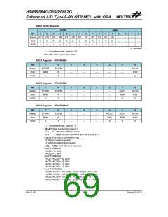
ADRH, ADRL Register
ADRH
ADRL
Bit
7
6
5
4
3
D7
R
2
1
D5
R
0
D4
R
7
D3
R
6
D2
R
5
4
D0
R
3
2
1
0
Name D11 D10 D9
D8
R
D6
R
D1
R
¾
¾
¾
¾
¾
¾
¾
¾
¾
¾
¾
¾
R/W
R
x
R
x
R
x
POR
x
x
x
x
x
x
x
x
x
²x² unknown
²¾² unimplemented, read as ²0²
D11~D0: ADC conversion data
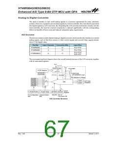
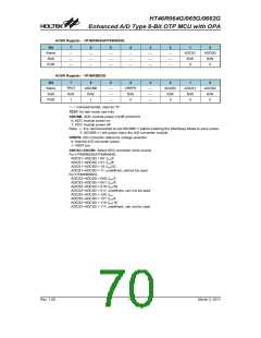
A/D Converter Control Registers - ADCR, ACSR, ANCSR
To control the function and operation of the A/D converter, these control registers known as ADCR,
ACSR and ANCSR are provided. These 8-bit registers define functions such as the selection of which
analog channel is connected to the internal A/D converter, which pins are used as analog inputs and
which are used as normal I/Os, the A/D clock source as well as controlling the start function and
monitoring the A/D converter end of conversion status.
The ACS2~ACS0 bits in the ADCR register define the channel number. As the device contains only
one actual analog to digital converter circuit, each of the individual 8 analog inputs must be routed to
the converter. It is the function of the ACS2~ACS0 bits in the ADCR register to determine which
analog channel is actually connected to the internal A/D converter.
The PCR7~PCR0 bits contained in the PCR or ANCSR register which determine which pins on
PC2~PC5 and PD4~PD7 are used as analog inputs for the A/D converter and which pins are to be used
as normal I/O pins. If the PCRn bit has a value of 1, then the corresponding pin, namely one of the
AN0~AN7 analog inputs, will be set as analog inputs. Note that if the PCRn bit is set to zero, then the
corresponding pin on PC2~PC5 and PD4~PD7 will be setup as a normal I/O pin for the HT46R0662G
device. However, for the HT46R064G and HT46R065G devices, if the PCRn bits are all set to zero,
the analog input channels will be all disabled and the A/D converter circuitry will be powered off.
Rev. 1.00
68
March 3, 2011

 HOLTEK [ HOLTEK SEMICONDUCTOR INC ]