HT46RU66/HT46CU66
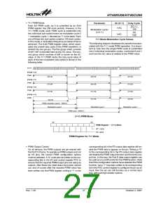
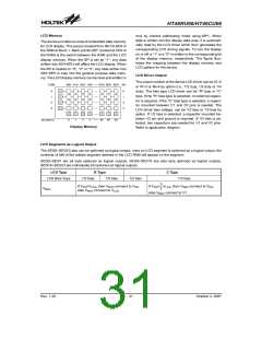
LCD Memory
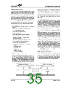
only by indirect addressing mode using MP1. When
data is written into the display data area, it is automati-
cally read by the LCD driver which then generates the
corresponding LCD driving signals. To turn the display
on or off, a ²1² or a ²0² is written to the corresponding bit
of the display memory, respectively. The figure illus-
trates the mapping between the display memory and
LCD pattern for the device.
The device provides an area of embedded data memory
for LCD display. This area is located from 40H to 6EH of
the RAM at Bank 1. Bank pointer (BP; located at 04H of
the RAM) is the switch between the RAM and the LCD
display memory. When the BP is set as ²1², any data
written into 40H~6EH will affect the LCD display. When
the BP is cleared to ²0², ²2² or ²3², any data written into
40H~6EH is map into the general purpose data mem-
ory. The LCD display memory can be read and written to
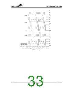
LCD Driver Output
The output number of the device LCD driver can be 47´2
or 47´3 or 46´4 by option (i.e., 1/2 duty, 1/3 duty or 1/4
duty). The bias type LCD driver can be ²R² type or ²C²
type. If the ²R² bias type is selected, no external capaci-
tor is required. If the ²C² bias type is selected, a capaci-
tor mounted between C1 and C2 pins is needed. The
LCD driver bias voltage can be 1/2 bias or 1/3 bias by
option. If 1/2 bias is selected, a capacitor mounted be-
tween V2 pin and ground is required. If 1/3 bias is se-
lected, two capacitors are needed for V1 and V2 pins.
Refer to application diagram.
C
O
M
4
0
H
4
1
H
4
2
H
4
3
H
6
C
H
6
D
H
6
E
H
B
i
t
0
1
2
3
0
1
2
3
S
E
G
M
E
N
T
0
1
2
3
4
4
4
5
4
6
Display Memory
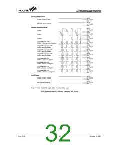
LCD Segments as Logical Output
The SEG0~SEG23 also can be optioned as logical output, once an LCD segment is optioned as a logical output, the
contents of bit0 of the related segment address in the LCD RAM will appear on the segment.
SEG0~SEG7 are all byte optioned as logical outputs, SEG8~SEG15 are also byte optioned as logical outputs,
SEG16~SEG23 are individually bit optioned as logical outputs.
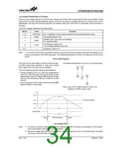
LCD Type
R Type
1/2 bias 1/3 bias
C Type
1/3 bias
LCD Bias Type
1/2 bias
3
2
If VDD
>
V
LCD, then VMAX connect to VDD
,
If VDD>VLCD, then VMAX connect to VDD,
else VMAX connect to VLCD
VMAX
else VMAX connect to V1
Rev. 1.20
31
October 2, 2007

 HOLTEK [ HOLTEK SEMICONDUCTOR INC ]