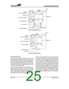
HT46RU66/HT46CU66
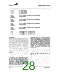
Bit No. Label
Function
Selects the A/D converter clock source
00=system clock/2
01=system clock/8
10=system clock/32
11=undefined
0
1
ADCS0
ADCS1
2~6
7
¾
Unused bit, read as ²0²
TEST For test mode used only
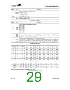
ACSR (27H) Register
Bit No. Label
Function
ACS2, ACS1, ACS0: Select A/D channel
0, 0, 0: AN0
0, 0, 1: AN1
0
1
2
ACS0 0, 1, 0: AN2
ACS1 0, 1, 1: AN3
ACS2 1, 0, 0: AN4
1, 0, 1: AN5
1, 1, 0: AN6
1, 1, 1: AN7
3
4
5
PCR0
Defines the Port B configuration select. If PCR0, PCR1 and PCR2 are all zero, the ADC circuit is
powered off to reduce power consumption.
PCR1
PCR2
Indicates end of A/D conversion. (0 = end of A/D conversion)
Each time bits 3~5 change state the A/D should be initialised by issuing a START signal, other-
wise the EOCB flag may have an undefined condition. See ²Important note for A/D initialisation².
6
7
EOCB
START
Starts the A/D conversion. (0®1®0= start; 0®1= Reset A/D converter and set EOCB to ²1²)
ADCR (26H) Register
PCR2
PCR1
PCR0
7
6
5
4
3
2
1
0
0
0
0
0
1
1
1
1
0
0
1
1
0
0
1
1
0
1
0
1
0
1
0
1
PB7
PB7
PB7
PB7
PB7
PB7
PB7
AN7
PB6
PB6
PB6
PB6
PB6
PB6
PB6
AN6
PB5
PB5
PB5
PB5
PB5
PB5
AN5
AN5
PB4
PB4
PB4
PB4
PB4
AN4
AN4
AN4
PB3
PB3
PB3
PB3
AN3
AN3
AN3
AN3
PB2
PB2
PB2
AN2
AN2
AN2
AN2
AN2
PB1
PB1
AN1
AN1
AN1
AN1
AN1
AN1
PB0
AN0
AN0
AN0
AN0
AN0
AN0
AN0
Port B Configuration
Register
Bit7
Bit6
Bit5
D1
Bit4
D0
Bit3
¾
Bit2
¾
Bit1
Bit0
¾
ADRL
ADRH
D3
D2
¾
D11
D10
D9
D8
D7
D6
D5
D4
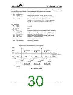
Note: D0~D11 is A/D conversion result data bit LSB~MSB.
ADRL (24H), ADRH (25H) Register
Rev. 1.20
29
October 2, 2007

 HOLTEK [ HOLTEK SEMICONDUCTOR INC ]