HT46RU66/HT46CU66
Low Voltage Reset/Detector Functions
There is a low voltage detector (LVD) and a low voltage reset circuit (LVR) implemented in this microcontroller. These
two functions can be enabled/disabled by options. Once the LVD option is enabled, the user can use the RTCC.3 to en-
able/disable (1/0) the LVD circuit and read the LVD detector status (0/1) from RTCC.5, otherwise, the LVD function is
disabled.
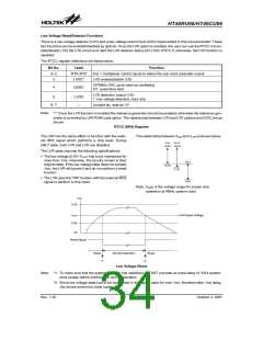
The RTCC register definitions are listed below.
Bit No.
0~2
3
Label
RT0~RT2
LVDC*
Function
8 to 1 multiplexer control inputs to select the real clock prescaler output
LVD enable/disable (1/0)
32768Hz OSC quick start-up oscillating
0/1: quick/slow start
4
QOSC
LVD detection output (1/0)
5
LVDO
1: low voltage detected, read only
6, 7
¾
Unused bit, read as ²0²
Note:
²*² Once the LVD function is enabled the reference generator should be enabled; otherwise the reference gen-
erator is controlled by LVR ROM code option. The relationship between LVR and LVD options and LVDC are as
shown.
RTCC (09H) Register
The LVR has the same effect or function with the exter-
nal RES signal which performs a chip reset. During
HALT state, both LVR and LVD are disabled.
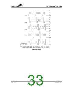
The relationship between VDD and VLVR is shown below.
V
D
D
V
O P R
5
.
5
V
5
.
5
V
The LVR state requires the following specifications:
·
The low voltage (0.9V~VLVR) has to be maintained for
more than 1ms, otherwise, the circuits remain in their
original state. If the low voltage state does not exceed
1ms, the LVR will ignore it and do not perform a reset
function.
V
L
V
R
3
.
0
V
2
.
2
V
·
The LVR uses the ²OR² function with the external RES
0
.
9
V
signal to perform a chip reset.
Note: VOPR is the voltage range for proper chip
operation at 4MHz system clock.
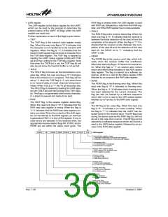
V
D
D
5
.
5
V
L
V
R
D
e
t
e
c
t
V
o
l
t
a
g
e
V
L
V
R
0
.
9
0
V
V
R
e
s
e
t
S
i
g
n
a
l
R
e
s
e
t
N
o
r
m
a
l
O
p
e
r
a
t
i
o
n
R
e
s
e
t
*
1
*
2
Low Voltage Reset
Note: *1: To make sure that the system oscillator has stabilized, the SST provides an extra delay of 1024 system
clock pulses before entering the normal operation.
*2: Since low voltage state has to be maintained in its original state for over 1ms, therefore after 1ms delay,
the device enters the reset mode.
Rev. 1.20
34
October 2, 2007

 HOLTEK [ HOLTEK SEMICONDUCTOR INC ]