HT46R51/HT46R52
Bit No.
Label
Function
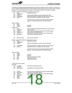
Defines the prescaler stages, PSC2, PSC1, PSC0=
000: fINT=fSYS
001: fINT=fSYS/2
0
1
2
PSC0 010: fINT=fSYS/4
PSC1 011: fINT=fSYS/8
PSC2 100: fINT=fSYS/16
101: fINT=fSYS/32
110: fINT=fSYS/64
111: fINT=fSYS/128
Defines the TMR active edge of the timer/event counter:
In Event Counter Mode (TM1,TM0)=(0,1):
1:count on falling edge;
3
TE
0:count on rising edge
In Pulse Width measurement mode (TM1,TM0)=(1,1):
1: start counting on the rising edge, stop on the falling edge;
0: start counting on the falling edge, stop on the rising edge
4
5
TON
Enable/disable timer counting (0=disable; 1=enable)
¾
Unused bit, read as ²0²
Defines the operating mode, TM1, TM0:
01=Event count mode (external clock)
10=Timer mode (internal clock)
11=Pulse width measurement mode
00=Unused
6
7
TM0
TM1
TMRC (0EH) Register
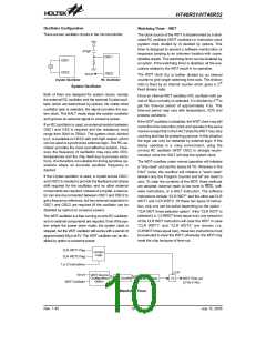
Input/Output Ports
There are 14 bidirectional input/output lines in the
microcontroller, labeled as PA, PB and PD, which are
mapped to the data memory of [12H], [14H] and [18H]
respectively. All of these I/O ports can be used for input
and output operations. For input operation, these ports
are non-latching, that is, the inputs must be ready at the
T2 rising edge of instruction ²MOV A,[m]² (m=12H, 14H
or 18H). For output operation, all the data is latched and
remains unchanged until the output latch is rewritten.
Each I/O line has its own control register (PAC, PBC,
PDC) to control the input/output configuration. With this
control register, CMOS output or Schmitt trigger input
with or without pull-high resistor structures can be re-
configured dynamically under software control. To func-
tion as an input, the corresponding latch of the control
register must write ²1². The input source also depends
on the control register. If the control register bit is ²1²,
the input will read the pad state. If the control register bit
V
D
D
C
o
n
t
r
o
l
B
i
t
P
U
D
Q
D
a
t
a
B
u
s
W
r
i
t
e
C
o
n
t
r
o
l
R
e
g
i
s
t
e
r
C
K
P
A
0
~
P
A
2
Q
P
P
P
P
P
P
P
A
A
A
A
A
B
D
3
4
5
6
7
0
/
/
/
P
T
I
F
D
S
C
h
i
p
R
e
s
e
t
M
R
N
T
R
e
a
d
C
o
n
t
r
o
l
R
e
g
i
s
t
e
r
D
a
t
a
B
i
t
/
A
N
0
~
P
B
4
/
A
N
4
D
C
Q
0
/
P
W
M
K
Q
W
r
i
t
e
D
a
t
a
R
e
g
i
s
t
e
r
S
M
U
X
M
E
N
(
P
F
D
o
r
P
W
M
)
[
P
A
3
,
P
F
D
]
U
o
r
[
P
D
0
,
P
W
M
]
X
R
e
a
d
D
a
t
a
R
e
g
i
s
t
e
r
S
y
s
t
e
m
W
a
k
e
-
u
p
(
P
A
o
n
l
y
)
W
a
k
e
-
u
p
I
N
T
f
o
r
P
A
5
O
n
l
y
Input/Output Ports
Rev. 1.40
14
July 12, 2005

 HOLTEK [ HOLTEK SEMICONDUCTOR INC ]