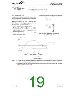
HT46R51/HT46R52
The PB can also be used as A/D converter inputs. The
A/D function will be described later. There is a PWM
function shared with PD0. If the PWM function is en-
abled, the PWM signal will appear on PD0 (if PD0 is op-
erating in output mode). The I/O functions of PD0 are as
shown.
is ²0², the contents of the latches will move to the inter-
nal bus. The latter is possible in the ²read-modify-write²
instruction.
For output function, CMOS is the only configuration.
These control registers are mapped to locations 13H,
15H and 19H.
I/O
I/P
O/P
I/P
O/P
After a chip reset, these input/output lines remain at high
levels or floating state (dependent on pull-high options).
Each bit of these input/output latches can be set or
cleared by ²SET [m].i² and ²CLR [m].i² (m=12H, 14H or
18H) instructions.
Mode (Normal) (Normal) (PWM)
(PWM)
Logical
Input
Logical
Output
Logical
Input
PD0
PWM
It is recommended that unused or not bonded out I/O
lines should be set as output pins by software instruction
to avoid consuming power under input floating state.
Some instructions first input data and then follow the
output operations. For example, ²SET [m].i², ²CLR
[m].i², ²CPL [m]², ²CPLA [m]² read the entire port states
into the CPU, execute the defined operations
(bit-operation), and then write the results back to the
latches or the accumulator.
PWM
The microcontroller provides one channel PWM output
shared with PD0. The PWM supports 6+2 mode. The
PWM channel has their data register denoted as
PWM(1AH). The frequency source of the PWM counter
comes from fSYS. The PWM register is an 8-bit register.
The waveforms of the PWM outputs are as shown.
Once the PD0 are selected as the PWM outputs and the
output function of the PD0 are enabled (PDC.0= ²0²),
writing ²1² to PD0 data register will enable the PWM out-
put function and writing ²0² will force the PD0 to stay at
²0².
Each line of port A has the capability of waking-up the
device. Each I/O port has a pull-high option. Once the
pull-high option is selected, the I/O port has a pull-high
resistor, otherwise, there¢s none. Take note that a non-
pull-high I/O port operating in input mode will cause a
floating state.
The PA3, PA4 and PA5 are pin-shared with PFD, TMR
and INT pins respectively.
If the PFD option is selected, the output signal in output
mode of PA3 will be the PFD signal generated by the
timer/event counter overflow signal. The input mode al-
ways remain in its original functions. Once the PFD op-
tion is selected, the PFD output signal is controlled by
the PA3 data register only. The I/O functions of PA3 are
shown below.
A (6+2) bits mode PWM cycle is divided into four modu-
lation cycles (modulation cycle 0~modulation cycle 3).
Each modulation cycle has 64 PWM input clock period.
In a (6+2) bit PWM function, the contents of the PWM
register is divided into two groups. Group 1 of the PWM
register is denoted by DC which is the value of
PWM.7~PWM.2. The group 2 is denoted by AC which is
the value of PWM.1~PWM.0. In a (6+2) bits mode PWM
cycle, the duty cycle of each modulation cycle is shown
in the table.
I/O
I/P
O/P
I/P
O/P
Mode (Normal) (Normal)
(PFD)
(PFD)
Logical
Input
Logical
Output
Logical
Input
PFD
PA3
(Timer on)
Parameter
AC (0~3) Duty Cycle
Note: The PFD frequency is the timer/event counter
overflow frequency divided by 2.
DC+1
i<AC
64
Modulation cycle i
(i=0~3)
The definitions of the PFD control signal and PFD output
frequency are listed in the following table.
DC
i³AC
64
Timer
PA3 Data PA3 Pad
Timer Preload
Value
Frequency
Register State
The modulation frequency, cycle frequency and cycle
duty of the PWM output signal are summarized in the
following table.
OFF
OFF
ON
X
X
N
N
0
1
0
1
0
U
X
X
PWM
PWM Cycle PWM Cycle
Duty
0
X
Modulation Frequency Frequency
ON
PFD
f
INT/(2´(256-N))
f
SYS/64 for (6+2) bits mode fSYS/256 [PWM]/256
Note:
²X² stands for ²unused²
²U² stands for ²unknown²
²N² is the preload value for the timer/event
counter
²fTMR² is the input clock frequency for the
timer/event counter
Rev. 1.40
15
July 12, 2005

 HOLTEK [ HOLTEK SEMICONDUCTOR INC ]