HT45R37
P
C
R
2
~
0
0
0
B
1
0
1
B
0
0
0
B
1
0
0
B
P
C
R
0
A
D
O
N
B
t
O
N
2
S
T
A
D
C
m
o
d
u
l
e
o
f
f
o
f
f
o
n
o
n
O
N
A
/
D
s
a
m
p
l
i
n
g
A
/
t
D
i
m
s
e
a
m
p
l
i
n
g
t
i
m
e
A
D
t
C
S
A
D
t
C
S
S
T
A
R
T
E
O
C
B
A
C
S
2
~
x
x
x
B
0
0
0
B
0
0
1
B
0
1
0
B
x
x
x
B
A
C
S
0
P
o
w
e
r
-
o
n
S
t
a
r
t
o
f
A
/
D
S
t
a
r
t
o
f
A
/
D
S
t
a
r
t
o
f
A
/
D
R
e
s
e
t
c
o
n
v
e
r
s
i
o
n
c
o
n
v
e
r
s
i
o
n
c
o
n
v
e
r
s
i
o
n
R
e
s
e
t
A
/
D
R
e
s
e
t
A
/
D
R
e
s
e
t
A
/
D
c
o
n
v
e
r
t
e
r
c
o
n
v
e
r
t
e
r
c
o
e
n
v
e
r
t
e
r
E
n
d
o
f
A
/
D
E
n
d
o
f
A
/
D
c
o
n
v
e
r
s
i
o
n
c
n
o
n
v
e
r
s
i
o
n
1
:
D
e
f
i
n
p
o
r
t
c
o
n
f
i
g
u
r
a
t
i
o
2
:
S
e
l
e
c
t
a
n
a
l
o
g
c
h
a
n
n
e
l
t
A
D
C
t
A
D
C
A
/
D
c
o
n
v
e
r
s
i
A
o
/
n
D
t
c
i
m
o
n
e
v
e
r
s
i
o
n
t
i
m
e
N
o
t
A
t
e
/
:
D
c
l
o
c
k
S
Y
/
m
S
2
S
u
,
Y
/
s
S
4
t
f
S
,
Y
/
b
S
8
f
S
e
,
Y
/
S
f
f
s
6
S
y
Y
/
s
o
S
3
,
r
2
f
f
A
A
D
D
=
C
C
S
4
A
D
t
t
=
A
D
t
+
C
S
n
A
*
;
D
t
n
=
b
i
t
c
o
u
n
t
o
f
A
D
C
r
e
s
o
l
u
t
i
o
n
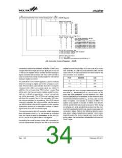
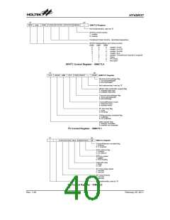
A/D Conversion Timing
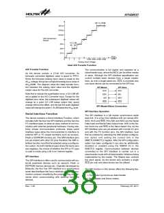
·
Step 5
internal hardware will begin to carry out the conversion,
during which time the program can continue with other
functions. The time taken for the A/D conversion is 16tAD
where tAD is equal to the A/D clock period.
If the interrupts are to be used, the interrupt control reg-
isters must be correctly configured to ensure the A/D
converter interrupt function is active. The master inter-
rupt control bit, EMI, in the INTC0 interrupt control reg-
ister must be set to ²1², the multi-function interrupt
enable bit, EMFI1, in the INTC1 register and the A/D
converter interrupt bit, EADI, in the MFIC1 register
must also be set to ²1².
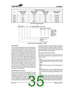
Programming Considerations
When programming, special attention must be given to
the A/D channel selection bits in the register. If these
bits are all cleared to zero no external pins will be se-
lected for use as A/D input pins allowing the pins to be
used as normal I/O pins. When this happens the power
supplied to the internal A/D circuitry will be reduced re-
sulting in a reduction of supply current. This ability to re-
duce power by turning off the internal A/D function by
clearing the A/D channel selection bits may be an impor-
tant consideration in battery powered applications. The
ADONB bit in the ACSR register can also be used to
power down the A/D function.
·
Step 6
The analog to digital conversion process can now be
initialised by setting the START bit in the ADCR regis-
ter from ²0² to ²1² and then to ²0² again. Note that this
bit should have been originally set to ²0².
·
Step 7
To check when the analog to digital conversion pro-
cess is complete, the EOCB bit in the ADCR register
can be polled. The conversion process is complete
when this bit goes low. When this occurs the A/D data
registers ADRL and ADRH can be read to obtain the
conversion value. As an alternative method if the in-
terrupts are enabled and the stack is not full, the pro-
gram can wait for an A/D interrupt to occur.
Another important programming consideration is that
when the A/D channel selection bits change value, the
A/D converter must be re-initialised. This is achieved by
pulsing the START bit in the ADCR register immediately
after the channel selection bits have changed state. The
exception to this is where the channel selection bits are
all cleared, in which case the A/D converter is not re-
quired to be re-initialised.
Note: When checking for the end of the conversion
process, if the method of polling the EOCB bit in
the ADCR register is used, the interrupt enable
step above can be omitted.
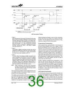
The accompanying diagram shows graphically the vari-
ous stages involved in an analog to digital conversion
process and its associated timing.
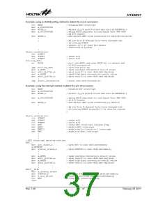
A/D Programming Example
The following two programming examples illustrate how
to setup and implement an A/D conversion. In the first
example, the method of polling the EOCB bit in the
ADCR register is used to detect when the conversion
cycle is complete, whereas in the second example, the
A/D interrupt is used to determine when the conversion
is complete.
The setting up and operation of the A/D converter func-
tion is fully under the control of the application program as
there are no configuration options associated with the
A/D converter. After an A/D conversion process has been
initiated by the application program, the microcontroller
Rev. 1.20
36
February 25, 2011
图片预览")
 HOLTEK [ HOLTEK SEMICONDUCTOR INC ]