HT45R37
Analog to Digital Converter
The need to interface to real world analog signals is a
common requirement for many electronic systems.
However, to properly process these signals by a
microcontroller, they must first be converted into digital
signals by A/D converters. By integrating the A/D con-
version electronic circuitry into the microcontroller, the
need for external components is reduced significantly
with the corresponding follow-on benefits of lower costs
and reduced component space requirements.
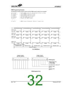
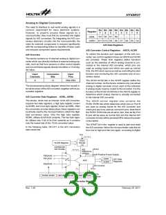
Bit Bit Bit Bit Bit Bit Bit Bit
Register
7
6
5
4
3
2
1
0
ADRL
D3 D2 D1 D0
¾
¾
¾
¾
ADRH D11 D10 D9 D8 D7 D6 D5 D4
A/D Data Registers
A/D Converter Control Registers - ADCR, ACSR
To control the function and operation of the A/D con-
verter, two control registers known as ADCR and ACSR
are provided. These 8-bit registers define functions
such as the selection of which analog channel is con-
nected to the internal A/D converter, which pins are
used as analog inputs and which are used as normal
I/Os, the A/D clock source as well as controlling the start
function and monitoring the A/D converter end of con-
version status.
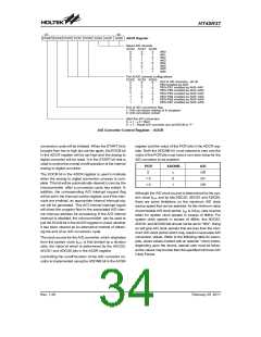
A/D Overview
The device contains an 6-channel analog to digital con-
verter which can directly interface to external analog sig-
nals, such as that from sensors or other control signals
and convert these signals directly into either a 12-bit dig-
ital value.
Input
Conversion
Bits
Input
Pins
Channels
6
12
PB0~PB5
The ACS2~ACS0 bits in the ADCR register define the
channel number. As the device contains only one actual
analog to digital converter circuit, each of the individual
6 analog inputs must be routed to the converter. It is the
function of the ACS2~ACS0 bits in the ADCR register to
determine which analog channel is actually connected
to the internal A/D converter.
The accompanying block diagram shows the overall in-
ternal structure of the A/D converter, together with its as-
sociated registers.
A/D Converter Data Registers - ADRL, ADRH
The device, which has an internal 12-bit A/D converter,
requires two data registers, a high byte register, known
as ADRH, and a low byte register, known as ADRL. After
the conversion process takes place, these registers can
be directly read by the microcontroller to obtain the digit-
ised conversion value. Only the high byte register,
ADRH, utilises its full 8-bit contents. The low byte regis-
ter utilises only 4 bit of its 8-bit contents as it contains
only the lowest bits of the 12-bit converted value.
The ADCR control register also contains the
PCR2~PCR0 bits which determine which pins on Port B
are used as analog inputs for the A/D converter and
which pins are to be used as normal I/O pins. Note that if
the PCR2~PCR0 bits are all set to zero, then all the Port
B pins will be setup as normal I/Os and the internal A/D
converter circuitry will be powered off to reduce the power
consumption.
The START bit in the register is used to start and reset
the A/D converter. When the microcontroller sets this bit
from low to high and then low again, an analog to digital
In the following table, D0~D11 is the A/D conversion
data result bits.
f
S
Y
S
C
l
o
c
k
A
C
S
R
R
e
g
i
D
s
i
t
v
e
i
r
d
e
r
¸
N
A
D
O
N
B
B
i
t
A
/
D
E
n
a
b
l
e
A
D
V
D
A
R
V
/
o
D
e
f
e
r
e
n
c
e
l
t
a
g
e
A
/
D
P
o
s
i
t
i
v
e
P
o
w
e
r
P
P
B
B
0
1
/
/
A
A
N
N
0
1
A
D
R
L
A
/
D
D
a
t
a
A
D
C
R
H
e
g
i
s
t
e
r
s
A
D
R
P
B
5
/
A
N
5
A
/
D
G
r
o
u
n
d
A
S
V
S
A
D
C
R
P
C
R
0
~
P
A
C
D
R
C
2
S
0
~
S
A
T
D
A
C
E
R
S
O
T
2
C
B
R
e
g
i
s
t
e
r
A/D Converter Structure
Rev. 1.20
33
February 25, 2011
图片预览")
 HOLTEK [ HOLTEK SEMICONDUCTOR INC ]