HT45R37
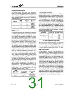
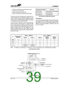
A/D Clock Period (tAD
)
ADCS2, ADCS1,
ADCS0=000
(fSYS/2)
ADCS2, ADCS1,
ADCS0=001
(fSYS/8)
ADCS2, ADCS1,
ADCS0=010
(fSYS/32)
ADCS2, ADCS1,
fSYS
ADCS0=011
1MHz
2MHz
4MHz
8MHz
12MHz
Undefined
Undefined
Undefined
Undefined
Undefined
2ms
8ms
4ms
32ms
16ms
8ms
1ms
500ns*
250ns*
167ns*
2ms
1ms
4ms
667ns*
2.67ms
A/D Clock Period Examples
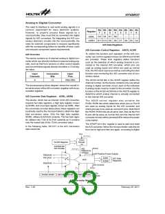
b
7
b
0
A
D
T
O
N
B
A
D
C
A
S
D
2
C
S
1
A
D
C
S
0
T
E
S
A
C
S
R
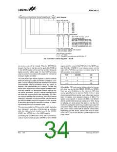
R
e
g
i
s
t
e
r
S
A
e
D
l
e
c
t
A
/
D
c
o
n
v
e
r
t
e
r
c
l
o
C
S
A
2
D
C
S
A
1
D
C
S
0
0
0
0
0
1
1
1
1
0
0
1
1
0
0
1
1
0
1
0
1
0
1
0
1
:
s
y
y
y
s
s
s
t
t
t
e
e
e
m
m
m
c
c
c
l
l
l
o
o
o
c
c
c
:
s
:
s
:
u
n
d
e
f
i
n
e
d
:
s
y
s
t
e
e
m
c
l
o
c
:
y
s
s
t
e
m
c
l
o
c
k
/
:
:
s
u
y
s
t
m
c
l
o
c
n
d
e
f
i
n
e
d
N
o
t
i
m
p
l
e
m
e
n
t
e
d
,
r
e
a
d
a
A
1
0
/
D
O
n
/
O
f
f
c
o
n
t
r
o
l
b
i
t
:
d
i
s
a
b
l
e
:
e
e
n
a
b
l
F
o
r
t
e
s
t
m
o
d
e
u
s
e
o
n
l
y
A/D Converter Control Register - ACSR
A/D Input Pins
the channel selection bits have changed, then, within a
time frame of one to ten instruction cycles, the START bit
in the ADCR register must first be set high and then im-
mediately cleared to zero. This will ensure that the EOCB
flag is correctly set to a high condition.
All of the A/D analog input pins are pin-shared with the
I/O pins on Port B. Bits PCR2~PCR0 in the ADCR regis-
ter, determine whether the input pins are setup as nor-
mal Port B input/output pins or whether they are setup
as analog inputs. In this way, pins can be changed under
program control to change their function from normal I/O
operation to analog inputs and vice versa. Pull-high re-
sistors, which are setup through register programming,
apply to the input pins only when they are used as nor-
mal I/O pins, if setup as A/D inputs the pull-high resistors
will be automatically disconnected. Note that it is not
necessary to first setup the A/D pin as an input in the
PBC port control register to enable the A/D input as
when the PCR2~PCR0 bits enable an A/D input, the sta-
tus of the port control register will be overridden. The
A/D converter has its own power supply pins AVDD and
AVSS pin. The analog input values must not be allowed
to exceed the value of AVDD.
Summary of A/D Conversion Steps
The following summarises the individual steps that
should be executed in order to implement an A/D con-
version process.
·
Step 1
Select the required A/D conversion clock by correctly
programming bits ADCS2, ADCS1 and ADCS0 in the
register.
·
Step 2
Enable the A/D by clearing the in the ACSR register to
zero.
·
Step 3
Select which channel is to be connected to the internal
A/D converter by correctly programming the
ACS2~ACS0 bits which are also contained in the reg-
ister.
Initialising the A/D Converter
The internal A/D converter must be initialised in a special
way. Each time the Port B A/D channel selection bits are
modified by the program, the A/D converter must be
re-initialised. If the A/D converter is not initialised after the
channel selection bits are changed, the EOCB flag may
have an undefined value, which may produce a false end
of conversion signal. To initialise the A/D converter after
·
Step 4
Select which pins on Port B are to be used as A/D in-
puts and configure them as A/D input pins by correctly
programming the PCR2~PCR0 bits in the ADCR reg-
ister. Note that this step can be combined with Step 2
into a single ADCR register programming operation.
Rev. 1.20
35
February 25, 2011
图片预览")
 HOLTEK [ HOLTEK SEMICONDUCTOR INC ]