HT45R37
¨
¨
¨
¨
LSB first or MSB first data transmission modes
Transmission complete flag
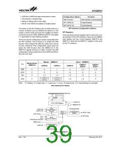
Configuration Option
SIM Function
Function
SIM interface enable/disable
Enable/Disable
Rising or falling active clock edge
SPI CSEN bit
WCOL and CSEN bit enabled or disable select
SPI WCOL bit
Enable/Disable
SPI Interface Configuration Options
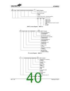
SPI Registers
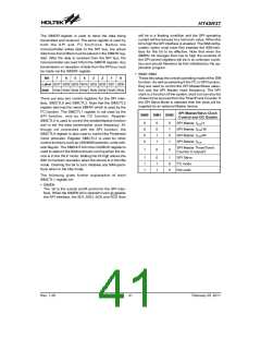
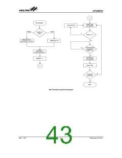
The status of the SPI interface pins is determined by a
number of factors such as whether the device is in the
master or slave mode and upon the condition of certain
control bits such as CSEN, SIMEN and SCS. In the table
I, Z represents an input floating condition.
There are three internal registers which control the over-
all operation of the SPI interface. These are the SIMDR
data register and two control registers SIMCTL0 and
SIMCTL2. Note that the SIMCTL1 register is only used
by the I2C interface.
There are several configuration options associated with
the SPI interface. One of these is to enable the SIM
function which selects the SIM pins rather than normal
I/O pins. Note that if the configuration option does not
select the SIM function then the SIMEN bit in the
SIMCTL0 register will have no effect. Another two SIM
configuration options determine if the CSEN and WCOL
bits are to be used.
Master - SIMEN=1
Slave - SIMEN=1
Master/Salve
Pin
CSEN=1
SCS=0
CSEN=1
SCS=1
SIMEN=0
CSEN=0
CSEN=1
CSEN=0
SCS
SDO
SDI
Z
Z
Z
Z
O
L
O
Z
O
I, Z
O
I, Z
Z
I, Z
I, Z
I, Z
I, Z
Z
H: CKPOL=0
L: CKPOL=1
H: CKPOL=0
L: CKPOL=1
SCK
Z
I, Z
I, Z
Z
Note:
²Z² floating, ²H² output high, ²L² output low, ²I² Input, ²O²output level, ²I,Z² input floating (no pull-high)
SPI Interface Pin Status
D
a
t
a
B
u
s
S
I
M
D
R
S
D
I
P
i
n
T
x
/
R
x
S
h
i
f
t
R
e
g
i
s
t
e
r
S
D
O
P
i
n
C
l
o
c
k
E
n
a
b
l
e
/
D
i
s
a
b
l
e
C
K
E
N
b
i
t
E
d
g
e
/
P
o
l
a
r
i
t
y
C
K
P
O
L
b
i
t
o
C
n
t
r
o
l
B
u
s
y
C
o
n
f
i
g
u
r
a
t
i
o
n
W
C
O
L
F
l
a
g
S
t
a
t
u
s
O
p
t
i
o
n
S
C
K
P
i
n
T
R
F
F
l
a
g
f
S
Y
S
C
l
o
c
k
f
S
U
B
S
o
u
r
c
e
S
e
l
e
c
t
T
i
m
e
r
/
E
v
e
n
t
C
o
u
n
t
e
r
S
C
S
P
i
n
C
o
n
f
i
g
u
r
a
t
i
o
n
C
S
E
N
b
i
t
O
p
t
i
o
n
E
n
a
b
l
e
/
D
i
s
a
b
l
e
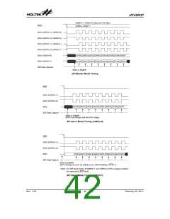
SPI Block Diagram
Rev. 1.20
39
February 25, 2011
图片预览")
 HOLTEK [ HOLTEK SEMICONDUCTOR INC ]