HT45R37
1
.
5
L
S
B
F
F
F
H
F
F
E
H
F
F
D
H
A
/
D
C
o
n
v
e
r
s
i
o
n
R
e
s
u
l
t
0
.
5
L
S
B
0
0
0
3
2
1
H
H
H
A
D
V
D
(
)
4
0
9
6
9
0
1
2
3
4
0
4
9
0
3
9
4
4
0
9
5
4
0
6
A
n
a
l
o
g
I
n
p
u
t
V
o
l
t
a
g
e
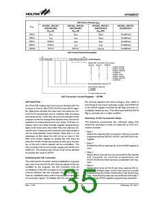
Ideal A/D Transfer Function
A/D Transfer Function
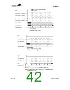
The communication is full duplex and operates as a
slave/master type, where the MCU can be either master
or slave. Although the SPI interface specification can
control multiple slave devices from a single master,
here, as only a single select pin, SCS, is provided only
one slave device can be connected to the SPI bus.
As the device contain a 12-bit A/D converter, its
full-scale converted digitised value is equal to FFFH.
Since the full-scale analog input value is equal to the
AVDD voltage, this gives a single bit analog input value of
AVDD/4096. The diagram show the ideal transfer func-
tion between the analog input value and the digitised
output value for the A/D converter.
S
P
I
M
a
s
t
e
S
r
P
I
S
l
a
v
e
S
C
K
S
S
S
S
C
D
D
C
K
I
O
S
Note that to reduce the quantisation error, a 0.5 LSB off-
set is added to the A/D Converter input. Except for the
digitised zero value, the subsequent digitised values will
change at a point 0.5 LSB below where they would
change without the offset, and the last full scale digitised
value will change at a point 1.5 LSB below the AVDD level.
S
D
O
S
D
I
S
C
S
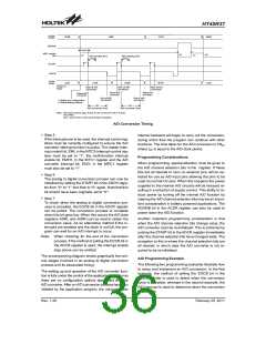
SPI Master/Slave Connection
SPI Interface Operation
Serial Interface Function
The SPI interface is a full duplex synchronous serial
data link. It is a four line interface with pin names SDI,
SDO, SCK and SCS. Pins SDI and SDO are the Serial
Data Input and Serial Data Output lines, SCK is the Se-
rial Clock line and SCS is the Slave Select line. As the
SPI interface pins are pin-shared with normal I/O pins
and with the I2C function pins, the SPI interface must
first be enabled by selecting the SIM enable configura-
tion option and setting the correct bits in the
SIMCTL0/SIMCTL2 register. After the SPI configuration
option has been configured it can also be additionally
disabled or enabled using the SIMEN bit in the
SIMCTL0 register. Communication between devices
connected to the SPI interface is carried out in a
slave/master mode with all data transfer initiations being
implemented by the master. The Master also controls
the clock signal. As the device only contains a single
SCS pin only one slave device can be utilised.
The device contains a Serial Interface Function, which
includes both the four line SPI interface and the two line
I2C interface types, to allow an easy method of commu-
nication with external peripheral hardware. Having rela-
tively simple communication protocols, these serial
interface types allow the microcontroller to interface to
external SPI or I2C based hardware such as sensors,
Flash or EEPROM memory, etc. The SIM interface pins
are pin-shared with other I/O pins therefore the SIM in-
terface function must first be selected using a configura-
tion option. As both interface types share the same pins
and registers, the choice of whether the SPI or I2C type
is used is made using a bit in an internal register.
SPI Interface
The SPI interface is often used to communicate with ex-
ternal peripheral devices such as sensors, Flash or
EEPROM memory devices etc. Originally developed by
Motorola, the four line SPI interface is a synchronous
serial data interface that has a relatively simple commu-
nication protocol simplifying the programming require-
ments when communicating with external hardware
devices.
The SPI function in this device offers the following fea-
tures:
¨
Full duplex synchronous data transfer
¨
Both Master and Slave modes
Rev. 1.20
38
February 25, 2011
图片预览")
 HOLTEK [ HOLTEK SEMICONDUCTOR INC ]