HT45R37
b
7
b
0
P
X
P
U
7
P
X
P
P
U
X
1
P
P
U
A
0
P
U
,
P
B
P
U
,
P
C
P
U
,
P
D
P
P
1
0
A
A
.
.
0
1
,
,
P
P
B
B
.
.
0
1
,
,
P
P
D
C
.
.
0
1
P
u
l
l
-
h
:
:
e
d
n
i
a
a
b
b
l
l
e
e
s
s
a
a
b
b
l
l
e
e
P
1
0
,
P
D
.
1
:
:
e
d
n
i
P
1
0
A
.
7
,
P
B
.
5
,
P
C
.
4
,
P
D
.
7
:
:
e
d
n
i
a
b
l
e
s
a
b
l
e
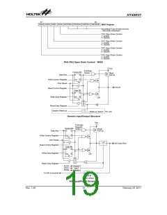
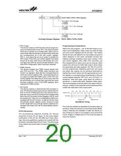
Pull-High Resistor Register - PAPU, PBPU, PCPU, PDPU
·
PFD Output
Programming Considerations
The device contains a PFD function whose single out-
put is pin-shared with I/O pin PA3. The output function
of this pin is chosen via a configuration option and re-
mains fixed after the device is programmed. Note that
the corresponding bit of the port control register,
PAC.3, must setup the pin as an output to enable the
PFD output. If the PAC port control register has setup
the pin as an input, then the pin will function as a nor-
mal logic input with the usual pull-high selection, even
if the PFD configuration option has been selected.
Within the user program, one of the first things to con-
sider is port initialisation. After a reset, all of the I/O data
and port control registers will be set high. This means
that all I/O pins will default to an input state, the level of
which depends on the other connected circuitry and
whether pull-high selections have been chosen. If the
port control registers, PAC, PBC, PCC and PDC, are
then programmed to setup some pins as outputs, these
output pins will have an initial high output value unless
the associated port data registers, PA, PB, PC and PD,
are first programmed. Selecting which pins are inputs
and which are outputs can be achieved byte-wide by
loading the correct values into the appropriate port con-
trol register or by programming individual bits in the port
control register using the ²SET [m].i² and ²CLR [m].i² in-
structions. Note that when using these bit control in-
structions, a read-modify-write operation takes place.
The microcontroller must first read in the data on the en-
tire port, modify it to the required new bit values and then
rewrite this data back to the output ports.
·
PWM Outputs
The device contains two PWM outputs shared with
pins PD0 and PD1. The PWM output functions are
chosen via registers. Note that the corresponding bit
of the port control register, PDC, must setup the pin as
an output to enable the PWM output. If the PDC port
control register has setup the pin as an input, then the
pin will function as a normal logic input with the usual
pull-high selection, even if the PWM registers have
enabled the PWM function.
·
A/D Inputs
The device contains a multi-channel A/D converter in-
puts. All of these analog inputs are pin-shared with I/O
pins on Port B. If these pins are to be used as A/D in-
puts and not as normal I/O pins then the corresponding
bits in the A/D Converter Control Register, ADCR, must
be properly set. There are no configuration options as-
sociated with the A/D function. If used as I/O pins, then
full pull-high resistor register remain, however if used
as A/D inputs then any pull-high resistor selections as-
sociated with these pins will be automatically discon-
nected.
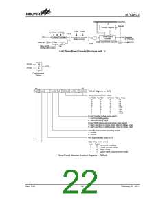
T
1
T
2
T
3
T
4
T
1
T
2
T
3
T
4
S
y
s
t
e
m
C
l
o
c
k
P
o
r
t
D
a
t
a
W
r
i
t
e
t
o
P
R
o
e
r
a
t
d
f
r
o
m
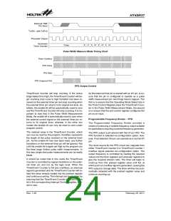
Read/Write Timing
Port A has the additional capability of providing wake-up
functions. When the device is in the Power Down Mode,
various methods are available to wake the device up.
One of these is a high to low transition of any of the Port
A pins. Single or multiple pins on Port A can be setup to
have this function.
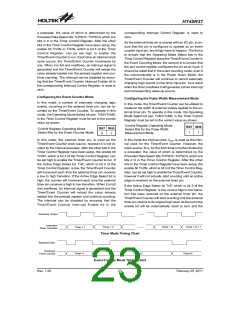
I/O Pin Structures
The accompanying diagrams illustrate the internal
structures of some I/O pin types. As the exact logical
construction of the I/O pin will differ from these draw-
ings, they are supplied as a guide only to assist with the
functional understanding of the I/O pins. The wide range
of pin-shared structures does not permit all types to be
shown.
Rev. 1.20
20
February 25, 2011
图片预览")
 HOLTEK [ HOLTEK SEMICONDUCTOR INC ]