HT45R37
In addition, on entering an interrupt sequence or execut-
ing a subroutine call, the status register will not be
pushed onto the stack automatically. If the contents of
the status registers are important and if the subroutine
can corrupt the status register, precautions must be
taken to correctly save it.
isters during normal program operation is a useful fea-
ture of these devices.
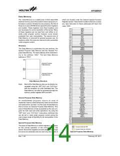
Pulse Width Modulator Registers
The devices contain two Pulse Width Modulator outputs
each with their own related independent control register
pair, known as PWM0L/PWM0H and PWM1L/ PWM1H.
The 12-bit contents of each register pair, which defines
the duty cycle value for the modulation cycle of the Pulse
Width Modulator, along with an enable bit are contained
in these register pairs.
Interrupt Control Registers
These 8-bit registers, known as the INTC0, INTC1,
MFIC0, MFIC1 and INTEDGE registers, control the op-
eration of the external and internal Timer/Event Counter
interrupt, Time Base interrupt, Real Time Clock inter-
rupt, A/D converter interrupt, C/R to F converter inter-
rupt and SPI/I2C interrupt. By setting various bits within
these registers using standard bit manipulation instruc-
tions, the enable/disable function of each interrupt can be
independently controlled. A master interrupt bit within this
register, the EMI bit, acts like a global enable/disable and
is used to set all of the interrupt enable bits on or off. This
bit is cleared when an interrupt routine is entered to dis-
able further interrupt and is set by executing the ²RETI²
instruction.
A/D Converter Registers - ADRL, ADRH, ADCR, ACSR
The device contains a multiple channel 12-bit A/D con-
verter. The correct operation of the A/D requires the use
of two data registers and two control registers. The two
data registers, a high byte data register known as
ADRH, and a low byte data register known as ADRL, are
the register locations where the digital value is placed
after the completion of an analog to digital conversion
cycle. Functions such as the A/D enable/disable, A/D
channel selection and A/D clock frequency are deter-
mined using the two control registers, ADCR and ACSR.
Timer/Event Counter Registers
C/R to F Converter Registers
The devices contains two 8-bit Timer/Event Counters.
The registers, TMR0 and TMR1 are the locations where
the timer values are located. These registers can also
be preloaded with fixed data to allow different time
intervals to be setup. The 8-bit Timer/Event Counters
have an associated control register, TMR0C and
TMR1C, which contain the setup information for these
timers, determines in what mode the timer is to be used
as well as containing the timer on/off control function.
The device contains a 16-channel C/R to F converter.
The correct operation of the C/R to F converter requires
the use of two 16-bit counters and five control registers.
The two 16-bit counters, a high byte register known as
TMRAH/TMRBH, and a low byte register known as
TMRAL/TMRBL. The channel selection of the C/R to F
converter is setup via the ASCR0~ASCR2 control regis-
ters. The configuration of the C/R to F converter is setup
via the RCOCCR or RCOCR control registers.
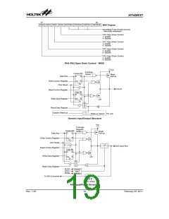
Input/Output Ports and Control Registers
Serial Interface Registers
Within the area of Special Function Registers, the I/O
registers and their associated control registers play a
prominent role. All I/O ports have a designated register
correspondingly labeled as PA, PB, PC and PD. These
labeled I/O registers are mapped to specific addresses
within the Data Memory as shown in the Data Memory
table, which are used to transfer the appropriate output
or input data on that port. With each I/O port there is an
associated control register labeled PAC, PBC, PCC and
PDC, also mapped to specific addresses with the Data
Memory. The control register specifies which pins of that
port are set as inputs and which are set as outputs. To
setup a pin as an input, the corresponding bit of the con-
trol register must be set high, for an output it must be set
low. During program initialization, it is important to first
setup the control registers to specify which pins are out-
puts and which are inputs before reading data from or
writing data to the I/O ports. One flexible feature of these
registers is the ability to directly program single bits us-
ing the ²SET [m].i² and ²CLR [m].i² instructions. The
ability to change I/O pins from output to input and vice
versa by manipulating specific bits of the I/O control reg-
The device contains two serial interfaces, an SPI and an
I2C interface. The SIMCTL0, SIMCTL1, SIMCTL2 and
SIMAR are the control registers for the Serial Interface
function while the SIMDR is the data register for the Se-
rial Interface Data.
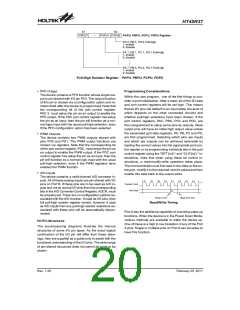
Port A Wake-up Register - PAWU
All pins on Port A have a wake-up function enable a low
going edge on these pins to wake-up the device when it
is in a power down mode. The pins on Port A that are
used to have a wake-up function are selected using this
resister.
Pull-High Resistors - PAPU, PBPU, PCPU, PDPU
All I/O pins on Ports PA, PB, PC and PD, if setup as in-
puts, can be connected to an internal pull-high resistor.
The pins which require a pull-high resistor to be con-
nected are selected using these registers.
Rev. 1.20
17
February 25, 2011
图片预览")
 HOLTEK [ HOLTEK SEMICONDUCTOR INC ]